
Semiconductor Device for Hybrid Energy Storage Systems

Active Publication Date: 2016-10-13
NEC CORP
View PDF0 Cites 26 Cited by
  • Summary
  • Abstract
  • Description
  • Claims
  • Application Information

AI Technical Summary

Benefits of technology

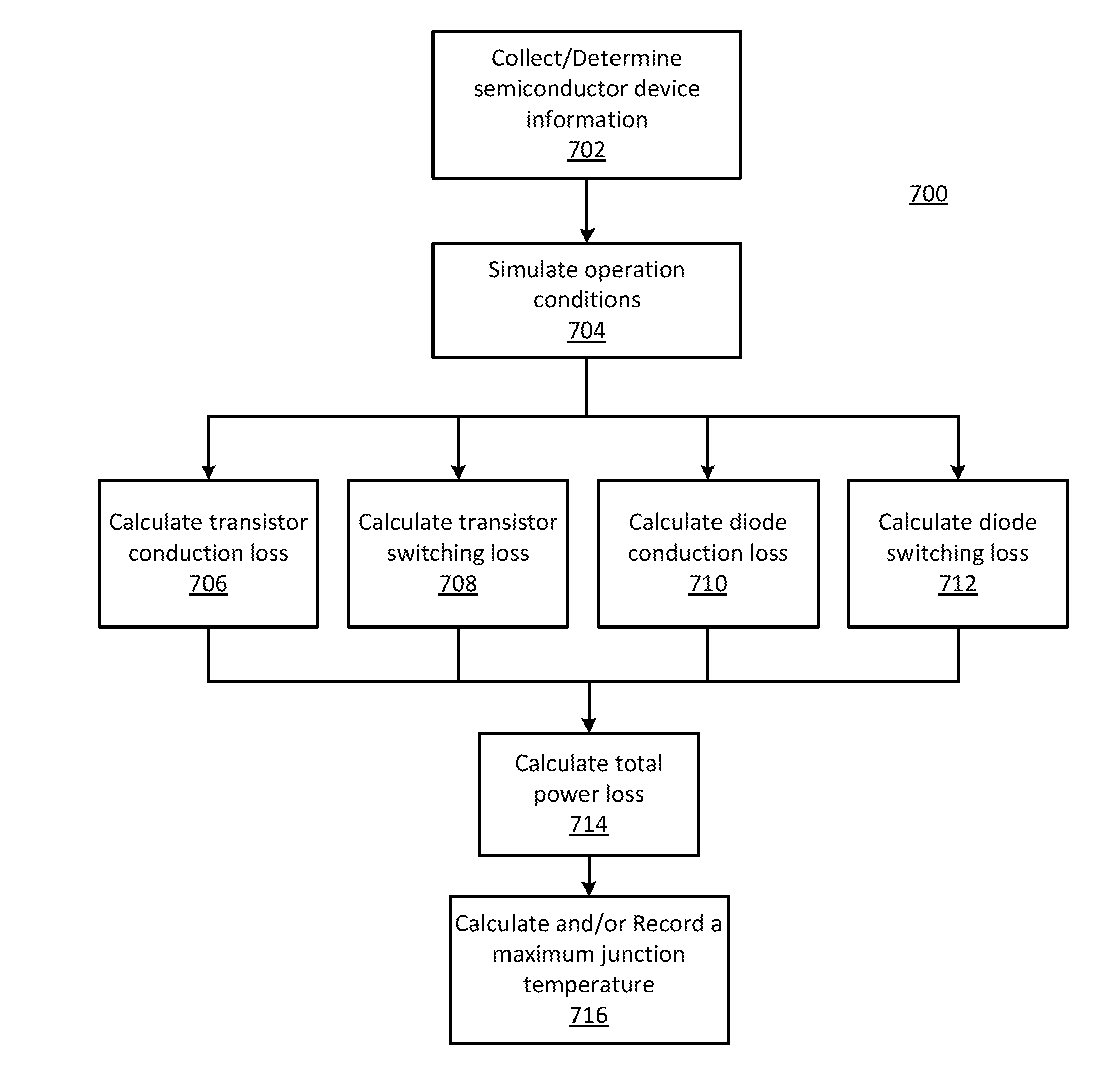
The patent describes a method for selecting semiconductor devices in a Modular Multilevel Converter (MMC) based on their performance under various operation conditions. This allows for the identification of the semiconductor device with the highest efficiency and the lowest cost. The method involves determining power losses and calculating maximum junction temperature for each semiconductor device under different operation conditions. The system then compares all semiconductor devices that meet a specific threshold voltage rating and a maximum junction temperature threshold condition to identify the most cost-effective solution. This approach can improve the overall performance and efficiency of the MMC system.

Problems solved by technology

However, single type energy storage elements cannot store a large amount of energy and provide high charging / discharging power, and as such, hybrid ESSs (HESSs) have been employed to utilize the advantages of different energy storage elements to provide a solution for this issue.
The addition of a dc / dc converter increases the system cost, and also introduces extra power loss.
Furthermore, with the increased power and energy ratings of the HESS for utility-level applications, the power semiconductor devices and passive components in these topologies may become unsuitable to handle the high voltage and current presented in the system.

Method used


Image

  • Semiconductor Device for Hybrid Energy Storage Systems
  • Semiconductor Device for Hybrid Energy Storage Systems
  • Semiconductor Device for Hybrid Energy Storage Systems

Examples


Embodiment Construction

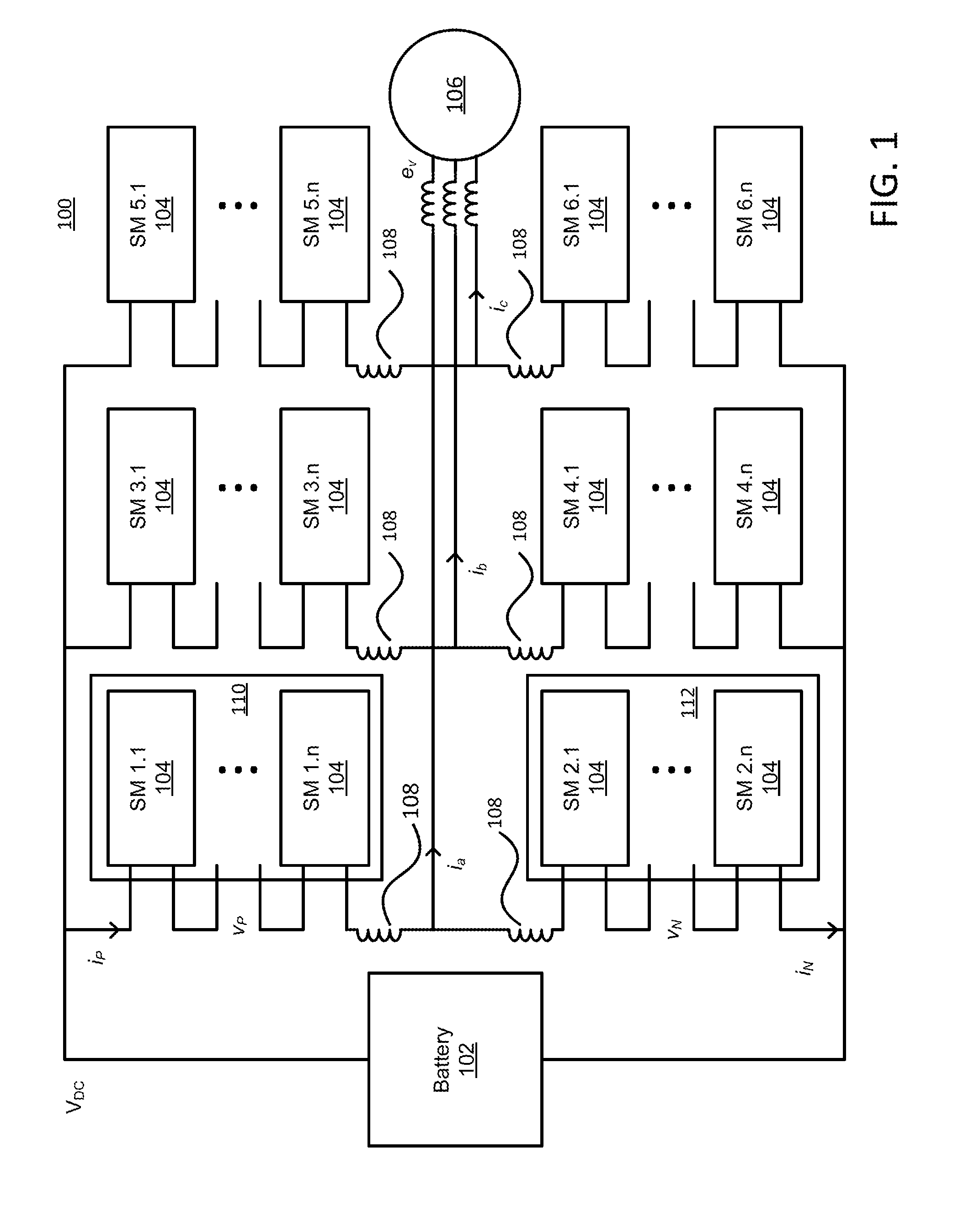
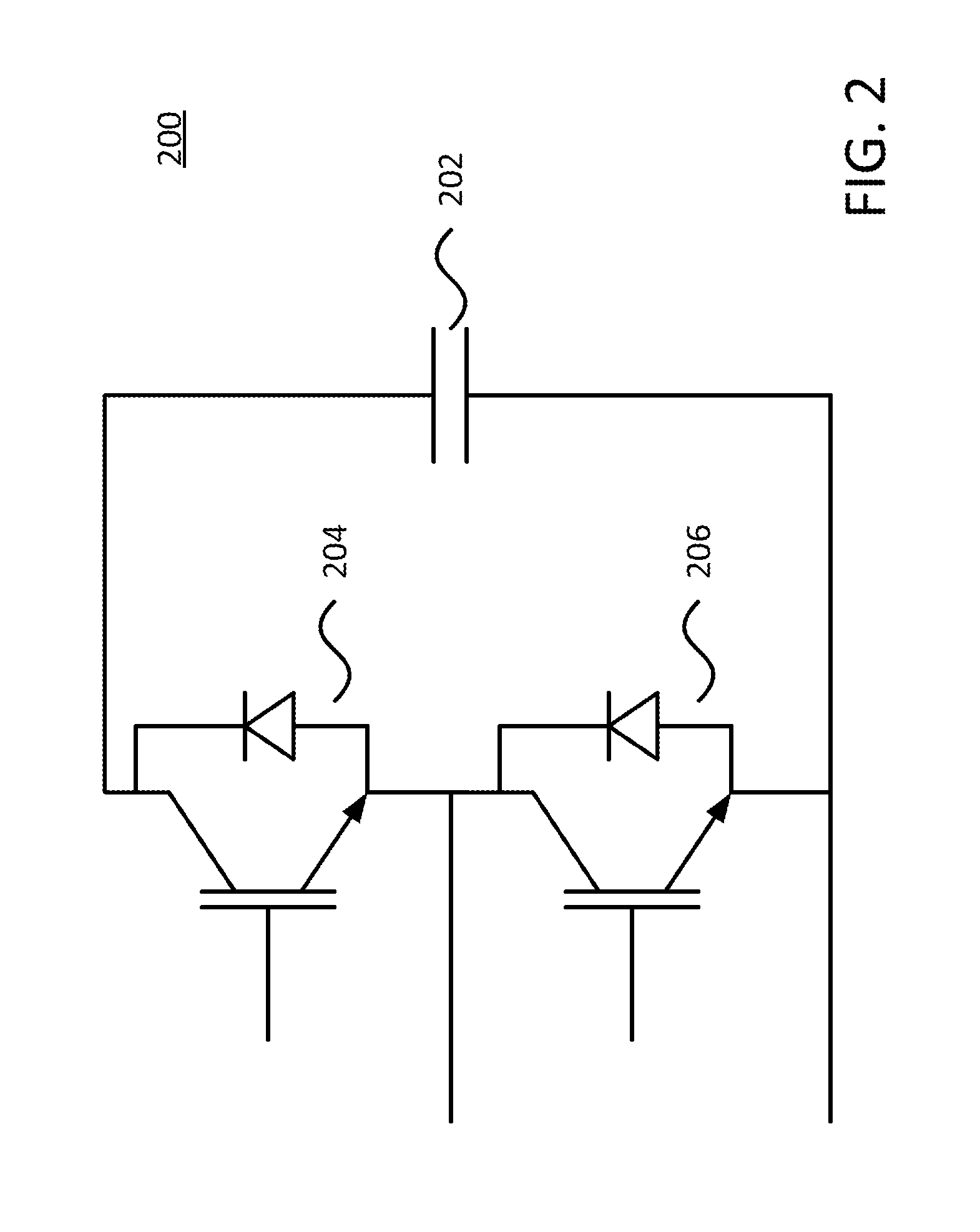
[0023]The present principles provide a system and method for semiconductor device selection for Modular Multilevel Converters (MMCs) and control frameworks for management of Energy Storage Systems (ESSs) (e.g., Hybrid ESSs (HESSs)), in accordance with various embodiments. In a particularly useful embodiment, semiconductor devices for MMCs in HESSs (which may combine a battery and an UltraCapacitor (UC)) may advantageously be selected based on ratings generated according to the present principles to maximize system efficiency and / or minimize system cost. In some embodiments, a two-layer control framework may be employed to control one or more HESSs according to the present principles.

[0024]As compared to conventional MMCs, embodiments of the present principles may have different principles of operation. Because of the integrated energy storage element, the average active power of each sub-module is not necessarily equal to zero and the power from the DC side is not necessarily equal ...


PUM


Abstract

Systems and methods for semiconductor device selection, including identifying a worst operation condition for a plurality of semiconductor devices in a Modular Multilevel Converter (MMC). The identifying includes determining power losses for each of the semiconductor devices under a plurality of operation conditions, and calculating a maximum junction temperature for each of the plurality of semiconductor devices at each of the plurality of operation conditions. A maximum junction temperature under the identified worst operation condition is determined for each of a plurality of commercially available semiconductor devices which satisfy a threshold voltage rating, and all semiconductor devices which satisfy the threshold voltage rating and a maximum junction temperature threshold condition are compared to identify a semiconductor device with a lowest system cost.

Description

RELATED APPLICATION INFORMATION[0001]This application claims priority to provisional application Ser. No. 62 / 144,632 filed on Apr. 8, 2015, incorporated herein by reference.BACKGROUND[0002]1. Technical Field[0003]The present invention relates to semiconductor device selection, and, more particularly, to semiconductor device selection for modular multilevel converters in energy storage systems.[0004]2. Description of the Related Art[0005]To support the penetration of renewable energy generation in the power grid and to provide ancillary functions for system operation (e.g., compensate for the fluctuation), the demand for energy storage systems (ESSs), which may store a large amount of energy and provide high charging / discharging power as needed, has increased. However, single type energy storage elements cannot store a large amount of energy and provide high charging / discharging power, and as such, hybrid ESSs (HESSs) have been employed to utilize the advantages of different energy s...

Claims


Application Information

Patent Timeline
IPC IPC(8): G01R31/36H02M7/537H02M1/08H02J1/00
CPCG01R31/3648H02J1/00H02M2001/0054H02M1/08H02M7/537G06N7/02H02M7/483G06F30/36G06F30/39G06F2119/08Y02B70/10H02M1/0054H02M7/4835G01R31/2601
Inventor GUO, FENGSHARMA, RATNESH
Owner NEC CORP
Learn More