Semiconductor device

Active Publication Date: 2016-10-27
RENESAS ELECTRONICS CORP
View PDF21 Cites 2 Cited by
  • Summary
  • Abstract
  • Description
  • Claims
  • Application Information

AI Technical Summary

Benefits of technology

The patent text explains a problem with normally-on junction FETs where the depletion layer narrows the effective source width and increases the on-resistance when there is no voltage applied to the gate layer. The technical effect of the patent is to improve the performance of semiconductor devices by reducing the on-resistance of the junction FET.

Problems solved by technology

As described above, it is difficult to achieve both of the improvement of the withstand voltage and the reduction of the on-resistance in the junction FET.
Therefore, it is difficult to achieve both of the improvement of the withstand voltage and the reduction of the on-resistance also in the semiconductor device having a junction FET and a MOSFET in cascode connection, and it is not possible to improve the characteristics of the semiconductor device.

Method used


Image

  • Semiconductor device
  • Semiconductor device
  • Semiconductor device

Examples


first embodiment

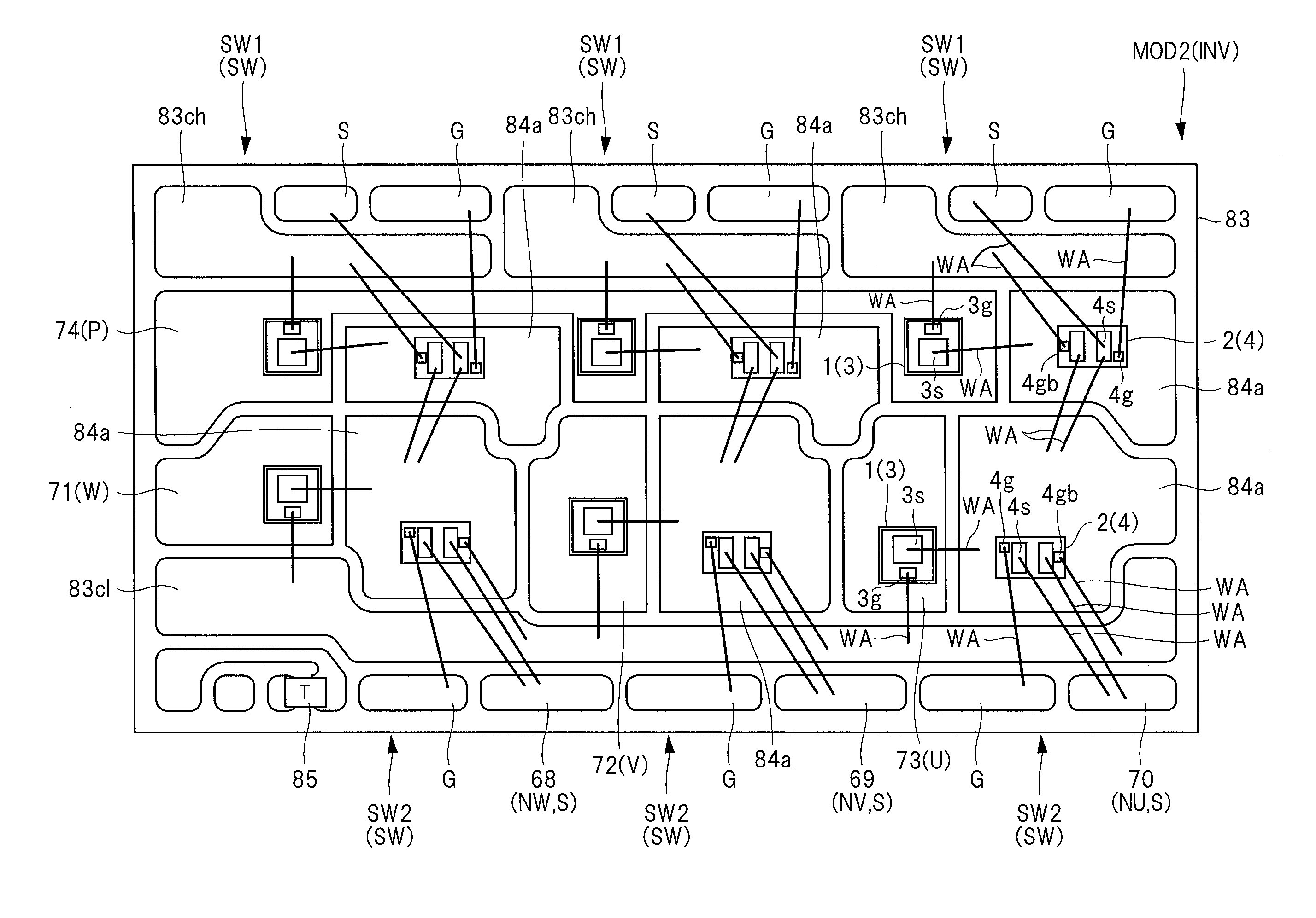
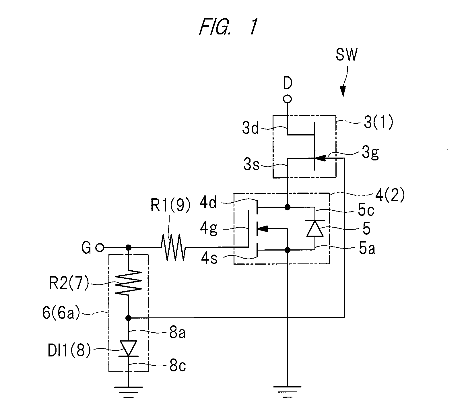
[0042]Hereinafter, a semiconductor device of the first embodiment will be described in detail with reference to drawings.

Circuit Configuration of Semiconductor Device

[0043]First, a circuit configuration of the semiconductor device of the first embodiment will be described. FIG. 1 and FIG. 2 are circuit diagrams each showing the configuration of the semiconductor device of the first embodiment.

[0044]As shown in FIG. 1, the semiconductor device includes a semiconductor chip 1, a semiconductor chip 2, a terminal G and a terminal D. A normally-on junction FET 3 is formed in the semiconductor chip 1, and a normally-off MOSFET 4 is formed in the semiconductor chip 2. The junction FET 3 has a gate electrode 3g, a source electrode 3s and a drain electrode 3d. The MOSFET 4 has a gate electrode 4g, a source electrode 4s and a drain electrode 4d. The junction FET 3 can be an n channel junction FET and the MOSFET 4 can be an n channel MOSFET.

[0045]In the specification of this application, a nor...

first modification example

of Semiconductor Device

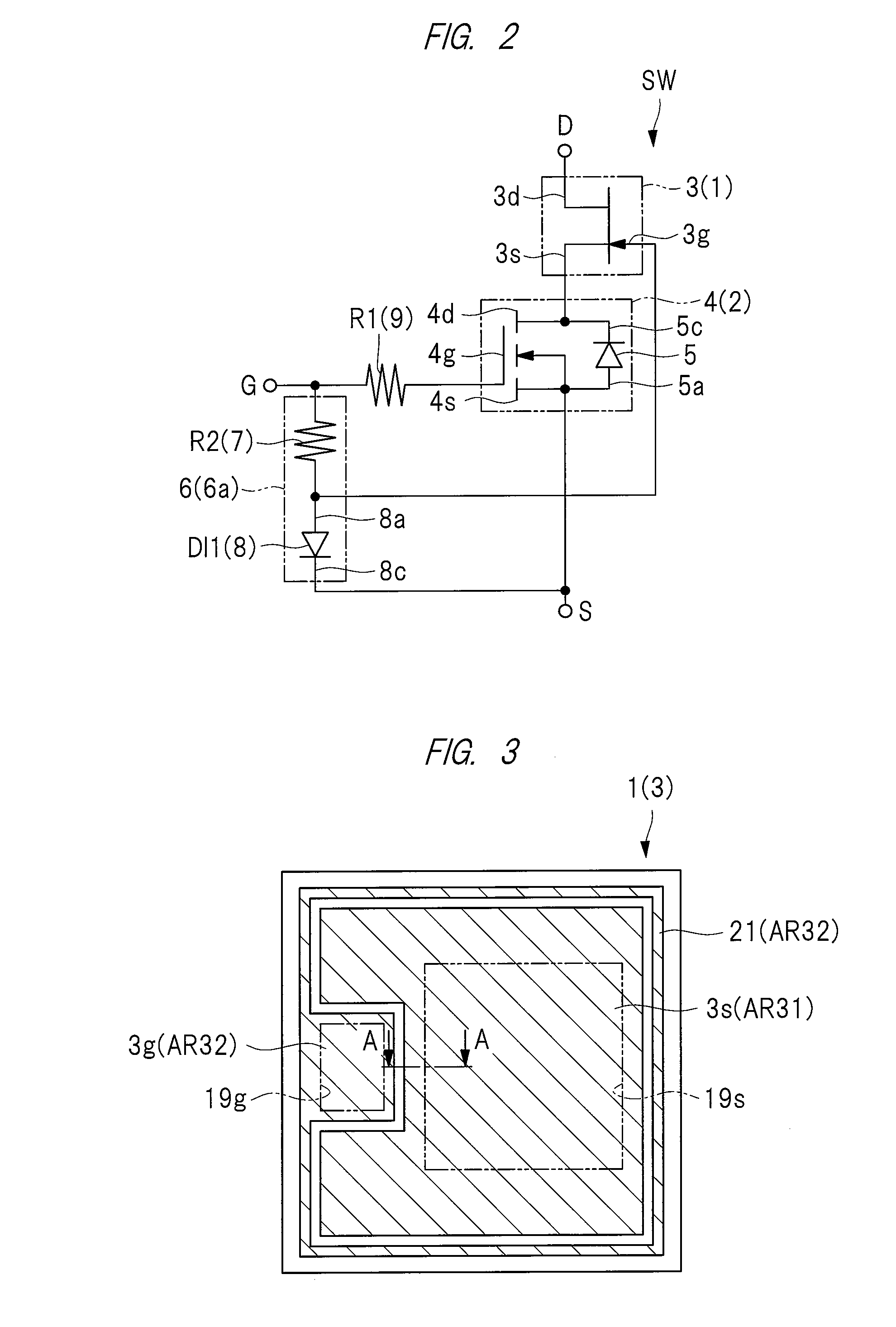
[0161]In the semiconductor device of the first embodiment, the voltage control element 6 includes the resistor R2 and the diode DI1, and the gate electrode 3g of the junction FET 3 is grounded through the diode DI1 or is electrically connected to the source electrode 4s of the MOSFET 4. Meanwhile, the voltage control element 6 may include only the resistor R2 but not include the diode DI1. The case like this will be described as the semiconductor device of the first modification example of the first embodiment. Note that the differences from the semiconductor device of the first embodiment will be mainly described below.

[0162]FIG. 14 is a circuit diagram of a configuration of the semiconductor device of the first modification example of the first embodiment.

[0163]As shown in FIG. 14, for example, the voltage control element 6, that is, the voltage applying unit 6a includes the resistor R2 but does not include the diode DI1 (see FIG. 1). The gate electrode 3g o...

second modification example

of Semiconductor Device of First Embodiment

[0167]In the semiconductor device of the first embodiment, the gate electrode 3g of the junction FET 3 is electrically connected to the gate electrode 4g of the MOSFET 4. Meanwhile, it is only required to apply a voltage with a polarity opposite to that of the voltage applied to the gate electrode 3g of the junction FET 3 to bring the junction FET 3 into an off-state, to the gate electrode 3g of the junction FET 3 when the MOSFET 4 is in an on-state. The case like this will be described as the semiconductor device of the second modification example of the first embodiment. Note that the differences from the semiconductor device of the first embodiment will be mainly described below.

[0168]FIG. 15 is a circuit diagram of a configuration of the semiconductor device of the second modification example of the first embodiment.

[0169]As shown in FIG. 15, the voltage control element 6 does not have to be electrically connected to the terminal G, tha...


PUM


Abstract

A semiconductor device includes a normally-on junction FET having a gate electrode, a source electrode and a drain electrode and a normally-off MOSFET having a gate electrode, a source electrode and a drain electrode. The source electrode of the junction FET is electrically connected to the drain electrode of the MOSFET, and the junction FET is thus connected to the MOSFET in series. The gate electrode of the junction FET is electrically connected to the gate electrode of the MOSFET.

Description

CROSS-REFERENCE TO RELATED APPLICATION[0001]The present application claims priority from Japanese Patent Application No. 2015-087671 filed on Apr. 22, 2015, the content of which is hereby incorporated by reference into this application.TECHNICAL FIELD OF THE INVENTION[0002]The present invention relates to a semiconductor device, and can be effectively applied to, for example, a power semiconductor device and a system using the power semiconductor device.BACKGROUND OF THE INVENTION[0003]A switching element made up of a field effect transistor (FET) with high operating voltage and being able to pass a large current, that is, a so-called power transistor has been widely used in, for example, power sources of an information device, home electronics and an in-vehicle device and a motor-drive device.[0004]A switching element using a cascode connection has been known as the switching element mentioned above. The switching element using a cascode connection includes, for example, a normally...

Claims


Application Information

Patent Timeline
IPC IPC(8): H01L25/18H02P27/06H01L23/00H01L29/10H01L25/07
CPCH01L25/18H01L29/1095H01L25/072H01L24/49H02P27/06H01L2224/48225H01L2924/13091H01L2924/10253H01L2924/10272H01L2924/1203H01L2924/1207H01L2924/13062H01L29/7827H01L29/808H03K17/04206H03K17/161H03K17/687H03K17/102H03K17/6871H03K17/74H03K2017/6875H01L2924/00014H01L2224/0603H01L2224/48137H01L2224/49113H01L24/48H01L2924/13055H01L2224/45015H01L2924/207H01L2224/45099H01L2924/00
Inventor TOYODA, HISASHIYAMAZAKI, KOICHIARAI, KOICHISEKI, TATSUHIRO
Owner RENESAS ELECTRONICS CORP
Why Eureka
Try Eureka