Organic light emitting diode

a light-emitting diode and organic technology, applied in the field of organic light-emitting diodes, can solve the problems of pixel shrinkage and lighting area reduction, and achieve the effect of reducing or eliminating pixel shrinkage and reducing lighting area over tim

Inactive Publication Date: 2016-11-10
BEIJING XIAOMI MOBILE SOFTWARE CO LTD
View PDF10 Cites 3 Cited by
  • Summary
  • Abstract
  • Description
  • Claims
  • Application Information

AI Technical Summary

Benefits of technology

[0004]It is an object of the present invention to reduce or eliminate pixel shrinkage, i.e., the reduction of the lighting area over time.

Problems solved by technology

One of the problems which conventional OLED lighting devices (as well as displays) face is pixel shrinkage, which involves the reduction of the lighting area over time due to deterioration of the functional layers.

Method used


Image

  • Organic light emitting diode
  • Organic light emitting diode
  • Organic light emitting diode

Examples


Embodiment Construction

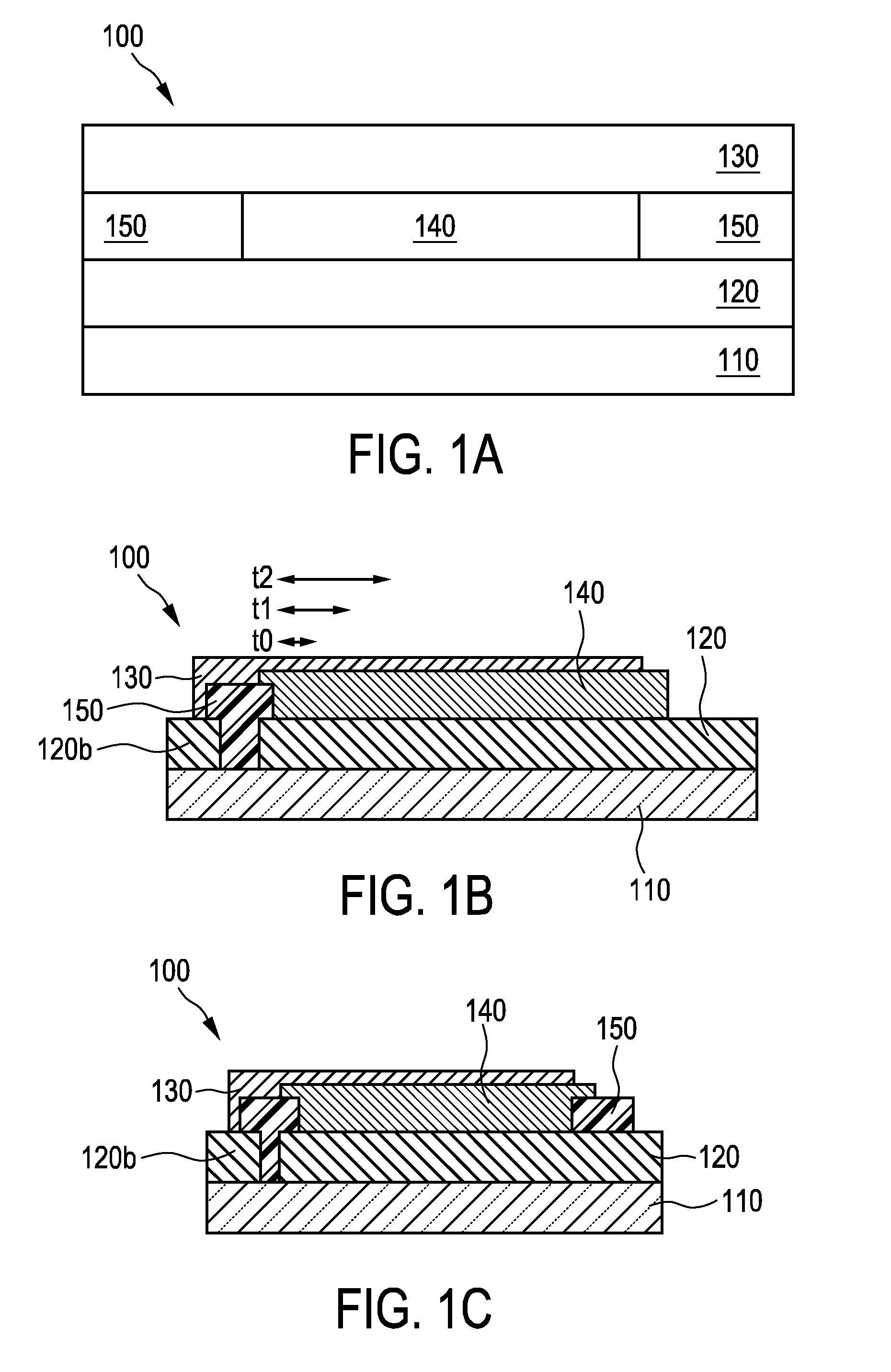
[0035]OLED substrates comprise a dielectric layer to provide an electrical isolation between the electrodes and to cover the edges of the electrodes which otherwise may lead to failure of the OLED device due to the high electric field at the edges of the electrodes and / or damaged organic layers resulting from edges of the shadow masks for the electrode layer. The dielectric layer also allows a certain degree of tolerance towards the misalignment of the mask during organic and cathode layer deposition.

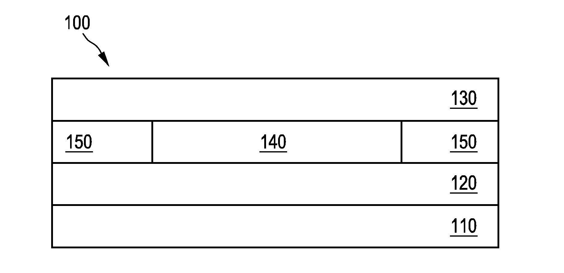
[0036]FIG. 1A shows schematically and exemplarily an embodiment of an organic light-emitting diode (OLED) 100. OLED 100 comprises a substrate 110, a first electrode 120, a second electrode 130, and an active layer 140 located in-between the first and second electrodes. Preferably, a dielectric layer 150 is locally placed to cover the edges of the organic / electrode layers 120, 130. In some embodiments (such as, e.g., the one illustrated in FIG. 1B), dielectric layer 150 may also cover th...


PUM


Abstract

The present invention relates to organic light emitting diodes (OLEDs) wherein organic photoresist layers are used as dielectric layers for electrical isolation. When organic photoresist layers are used as dielectric layers in OLEDs, a problem called “pixel shrinkage” may occur. According to the invention, the problem of pixel shrinkage can be solved by using an acrylic resin such as methyl methacrylate or a solution of polyimide in gamma-butyrolactone to form the dielectric layer. There is provided an organic light emitting diode (100) comprising: a substrate layer (110); a first electrode layer (120); a second electrode layer (130); an active layer (140) in-between the first and second electrode layers (120, 130); and a dielectric layer (150) configured to provide an electrical isolation between the first and second electrodes (120, 130). The dielectric layer (150) comprises a dielectric material configured to produce a reduced amount of or no by-products during a curing process.

Description

FIELD OF THE INVENTION[0001]The invention relates to an organic light emitting diode, a fabrication apparatus for fabricating an organic light emitting diode, and a fabrication method for fabricating an organic light emitting diode.BACKGROUND OF THE INVENTION[0002]US-2013 / 009162-A1 discloses an organic light-emitting display device including a substrate; a plurality of thin film transistors (TFTs) on the substrate; a plurality of first electrodes respectively on the TFTs; a pixel-defining layer between the first electrodes, the pixel-defining layer including a covered portion and an uncovered portion; a plurality of organic layers respectively on the first electrodes, each organic layer including an emission layer; a second electrode covering at least a part of the organic layers and the pixel-defining layer, a portion of the pixel-defining layer covered by the second electrode defining the covered portion, wherein at least one outgassing hole is in the uncovered portion of the pixe...

Claims


Application Information

Patent Timeline
Patent Type & Authority Applications(United States)
IPC IPC(8): H01L27/32H01L51/50H01L51/56H01L51/52
CPCH01L27/3246H01L51/5206H01L51/5221H01L2227/323H01L51/56H01L2251/308H01L2251/301H01L51/5012H10K59/173H10K59/122H10K50/11H10K50/81H10K50/82H10K71/00H10K59/1201H10K2102/00H10K2102/103
Inventor MOHANAN, SENTHILNATHANRICKERS, CHRISTOPHWENDELS, MARCHARTMANN, SOEREN
Owner BEIJING XIAOMI MOBILE SOFTWARE CO LTD
Why Eureka
Try Eureka