Amoled backplane structure and manufacturing method thereof

a backplane and amoled technology, applied in the field of amoled backplane structure, can solve the problems of reducing resolution, accelerating aging of oled materials, design difficulty, etc., and achieve the effects of ensuring smoothness of a planarization layer, increasing the effective displaying area, and prolonging the life of an oled

Active Publication Date: 2016-11-17
SHENZHEN CHINA STAR OPTOELECTRONICS TECH CO LTD
View PDF16 Cites 10 Cited by
  • Summary
  • Abstract
  • Description
  • Claims
  • Application Information

AI Technical Summary

Benefits of technology

[0008]An object of the present invention is to provide an active matrix organic light emitting display (AMOLED) backplane structure, which helps ensure smoothness of a planarization layer without an abrupt change site and also makes a pixel electrode in the form of a curved configuration so as to increase an effective displaying area, extend a lifespan of an OLED, reduce the difficulty of manufacturing, and enhance resolution.

Problems solved by technology

This leads to accelerated aging of the OLED material.
This leads to problems of design difficulty and reduction of resolution.
However, in the above-discussed patent document, the planarization layer 304 and the curved sections 304a are formed at the same time and there would be a potential risk that defects may occur in GD at abrupt change sites and thus affect the lifespan of the OLED.
In addition, manufacturing of the curved sections 304a requires the use of gray scale masks; this increases the difficulty of the process and leads to deterioration of yield rate.

Method used


Image

  • Amoled backplane structure and manufacturing method thereof
  • Amoled backplane structure and manufacturing method thereof
  • Amoled backplane structure and manufacturing method thereof

Examples


first embodiment

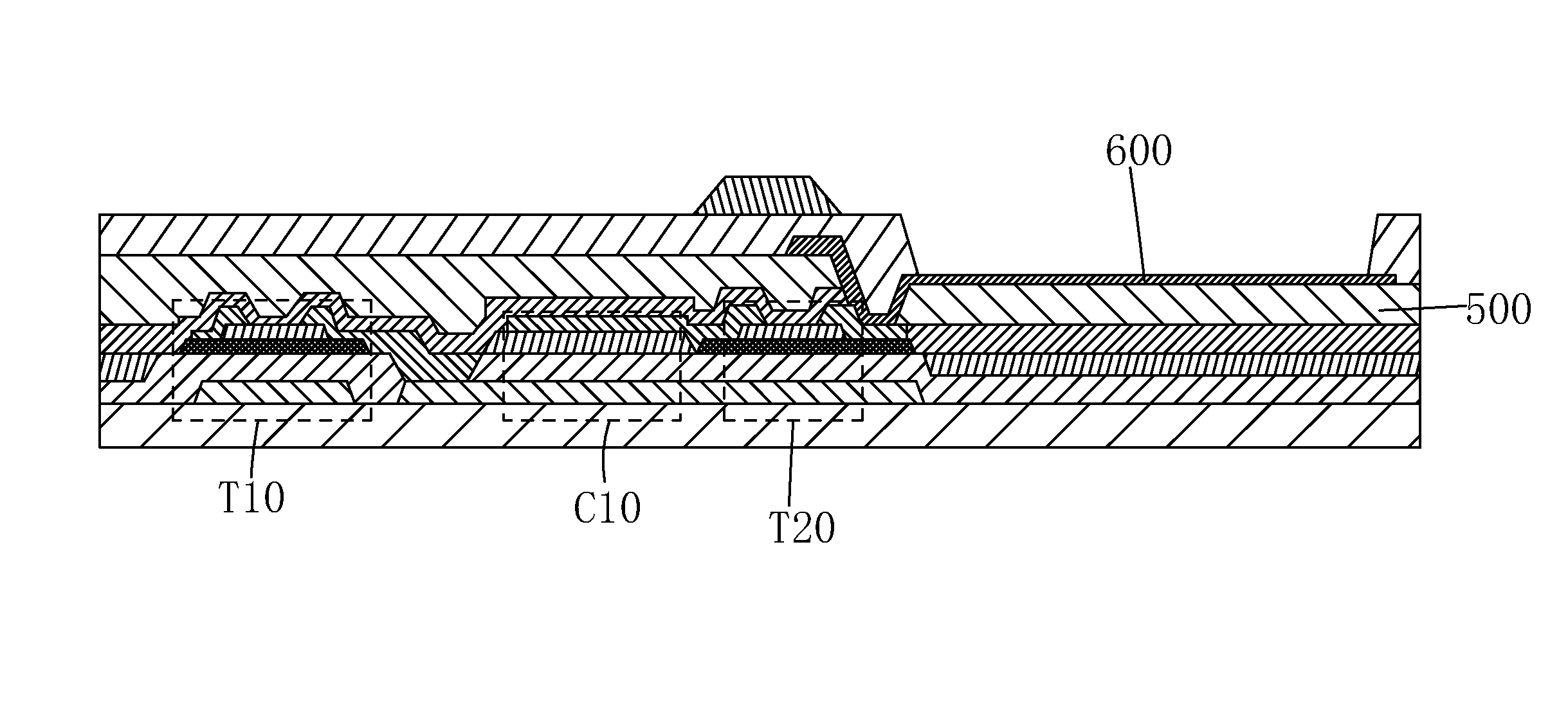
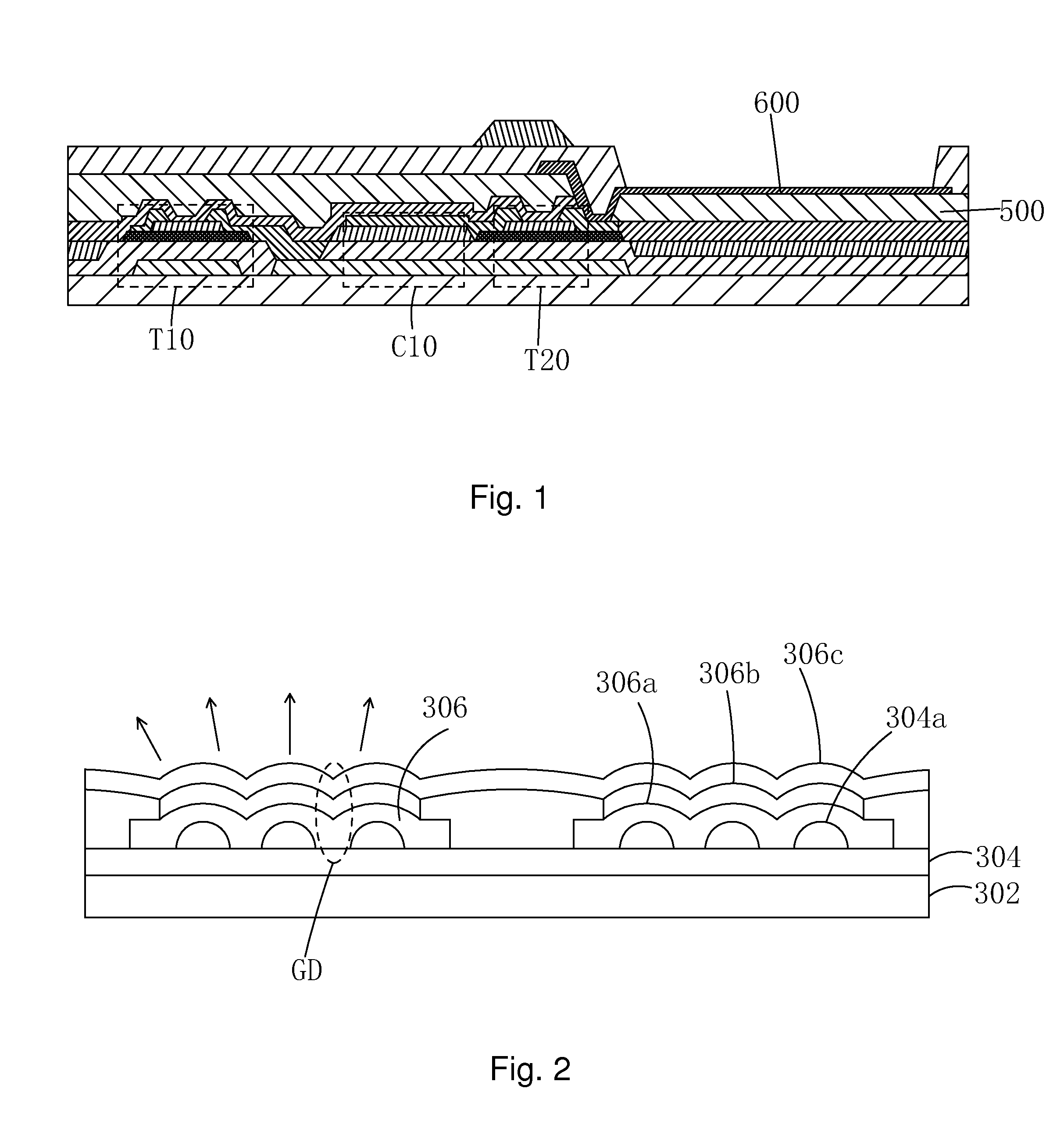
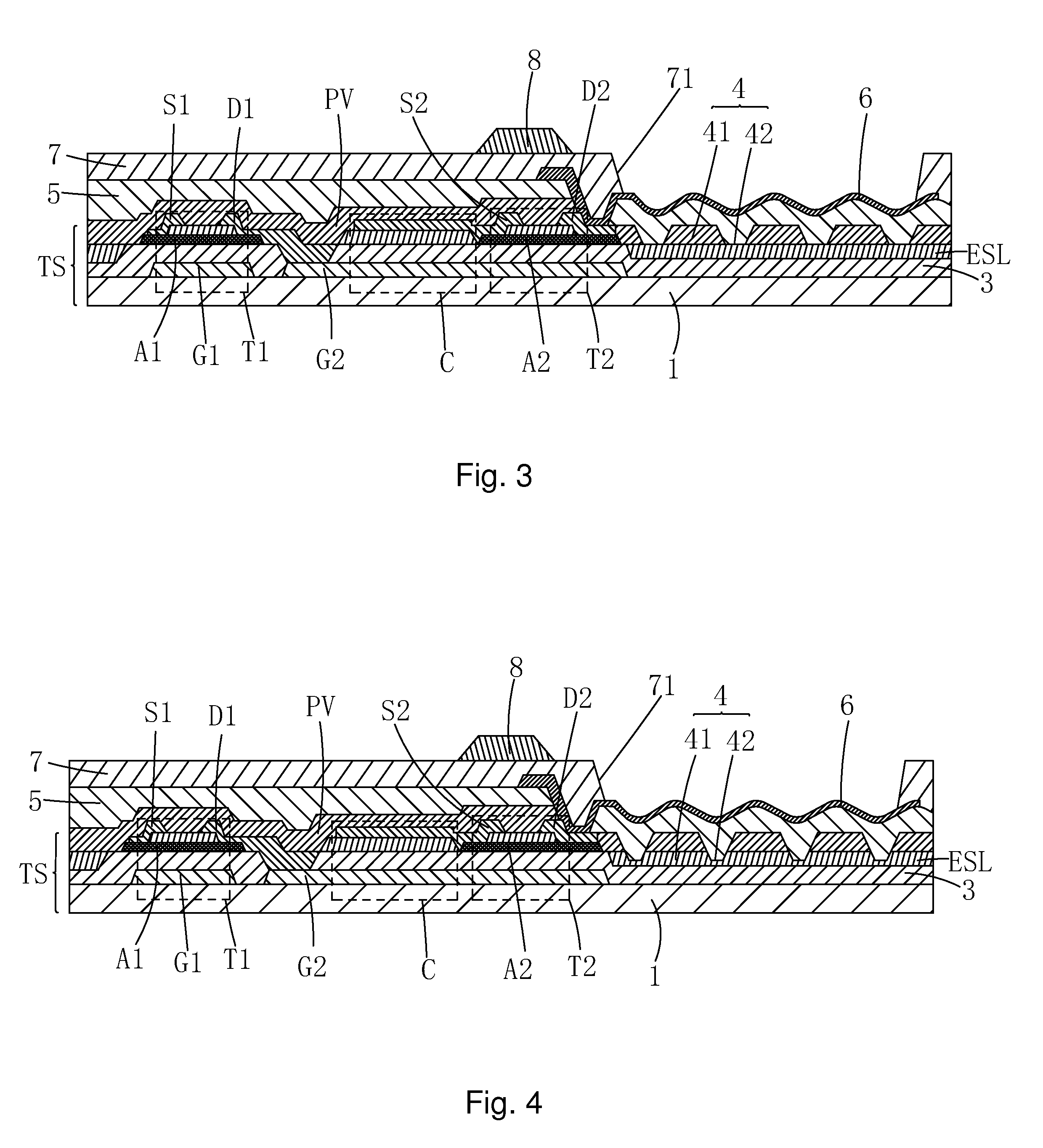
[0052]Firstly, the present invent provides an AMOLED backplane structure. Referring to FIG. 3, an AMOLED backplane structure according to the present invention is shown, which comprises multiple sub-pixels arranged in an array. In each of the sub-pixels, the AMOLED backplane comprises: a thin-film transistor (TFT) substrate TS, a planarization layer 5 formed on the TFT substrate TS, a pixel electrode 6 formed on the planarization layer 5, a pixel definition layer 7 formed on the pixel electrode 6, and a photo spacer 8 formed on the pixel definition layer 7.

[0053]The TFT substrate TS comprises therein a switch TFT T1, a drive TFT T2, and a capacitor C.

[0054]The pixel definition layer 7 comprises an opening 71 formed therein to expose a portion of the pixel electrode 6.

[0055]The TFT substrate TS comprises a corrugation structure 4 arranged in an area corresponding to the opening 71 of the pixel definition layer 7. The corrugation structure 4 comprises a plurality of raised sections 41...

second embodiment

[0066]For the AMOLED backplane structure of the second embodiment shown in FIG. 4, in Step 1, in the same time of forming a protective layer PV, the protective layer PV and an etch stop layer ESL are both subjected to dry etching to form the corrugation structure 4.

third embodiment

[0067]For the AMOLED backplane structure of the third embodiment shown in FIG. 5, in Step 1, in the same time of forming first source and drain terminals S1, D1 and second source and drain terminals S2, D2, a metal layer M is subjected to dry etching to form the corrugation structure 4.

[0068]Step 2: as shown in FIG. 6, with the AMOLED backplane structure of the first embodiment shown in FIG. 3 being taken as an example, coating organic photoresist on the TFT substrate TS that comprises the corrugation structure 4 formed thereon to form a planarization layer 5 in such a way that an upper surface of a portion of the planarization layer 5 corresponding to and located above the corrugation structure 4 comprises a curved configuration corresponding to the corrugation structure 4 in order to ensure smoothness of the planarization layer and thus being free of abrupt change site.

[0069]In Step 2, the organic photoresist is directly coated to form the planarization layer 5 without a gray scal...


PUM


Abstract

The present invention provides an AMOLED backplane structure and a manufacturing method thereof. In each sub-pixel, a TFT substrate (TS) includes a corrugation structure (4) formed in an area corresponding to an opening (71) of a pixel definition layer (7). The corrugation structure (4) includes a plurality of raised sections (41) and a recessed section (42) formed between every two adjacent ones of the raised sections (41). An upper surface of a portion of the planarization layer (5) and a portion of a pixel electrode (6) that correspond to and are located above the corrugation structure (4) include curved surfaces corresponding to the corrugation structure (4). The AMOLED backplane structure helps ensure the planarization layer (5) is smooth and free of abrupt change sites and also makes the pixel electrode (6) in a form of a curved surface to increase an effective displaying surface, extend the lifespan of the OLED, reduce difficulty of manufacturing, and improve resolution.

Description

BACKGROUND OF THE INVENTION[0001]1. Field of the Invention[0002]The present invention relates to the field of displaying technology, and in particular to an active matrix organic light emitting display (AMOLED) backplane structure and a manufacturing method thereof.[0003]2. The Related Arts[0004]An organic light emitting display (AMOLED) is a displaying technique having a extremely prosperous future. An OLED display device shows excellent displaying performance and also possesses various advantages, such as being self-luminous, simple structure, being ultra-thin and light, fast response speed, wide view angle, low power consumption, and being capable of achieving flexible displaying and is thus regarded as a “dream display” that attracts the attention of major display manufacturers and becomes the mainstream of the three-generation display devices of the field of display technology.[0005]The OLED display devices are classified, according to the way of driving, into two categories, i...

Claims


Application Information

Patent Timeline
Patent Type & Authority Applications(United States)
IPC IPC(8): H01L27/32H01L51/52H01L51/56H01L29/45
CPCH01L27/3258H01L27/3211H01L27/3262H01L27/3246H01L27/3265H01L2227/323H01L51/5206H01L51/56H01L27/1248H01L27/1255H01L2251/308H01L29/45H10K59/35H10K59/124H10K50/813H10K50/81H10K59/122H10K59/1213H10K59/1216H10K71/00H10K59/1201H10K2102/103H01L27/1262
Inventor LI, WENHUIWANG, YIFAN
Owner SHENZHEN CHINA STAR OPTOELECTRONICS TECH CO LTD
Why Eureka
Try Eureka