Semiconductor device

Inactive Publication Date: 2016-11-17
UNISANTIS ELECTRONICS SINGAPORE PTE LTD
View PDF3 Cites 5 Cited by
  • Summary
  • Abstract
  • Description
  • Claims
  • Application Information

AI Technical Summary

Benefits of technology

[0032]Therefore, when the silicide is formed in an upper portion of a silicon column, a hole is formed on a polysilicon gate electrode after the polysilicon gate is formed, the silicide is formed after a side wall composed of an insulating film is formed on the side wall of the hole, and then the hole is filled with an insulating film, thereby causing the problem of increasing the number of manufacturing steps. Therefore, the diffusion layers are formed before the polysilicon gate electrode and the polysilicon gate

Problems solved by technology

Finer MOS transistors have the problem of difficulty in suppressing leak currents and difficulty in dec

Method used


Image

  • Semiconductor device
  • Semiconductor device
  • Semiconductor device

Examples


Embodiment Construction

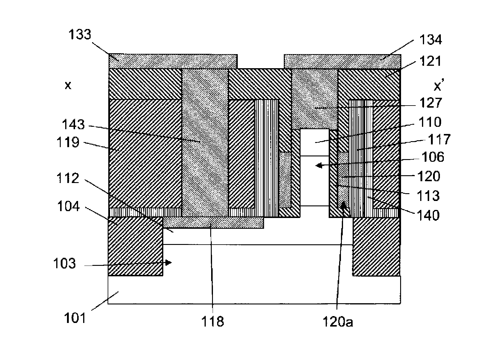
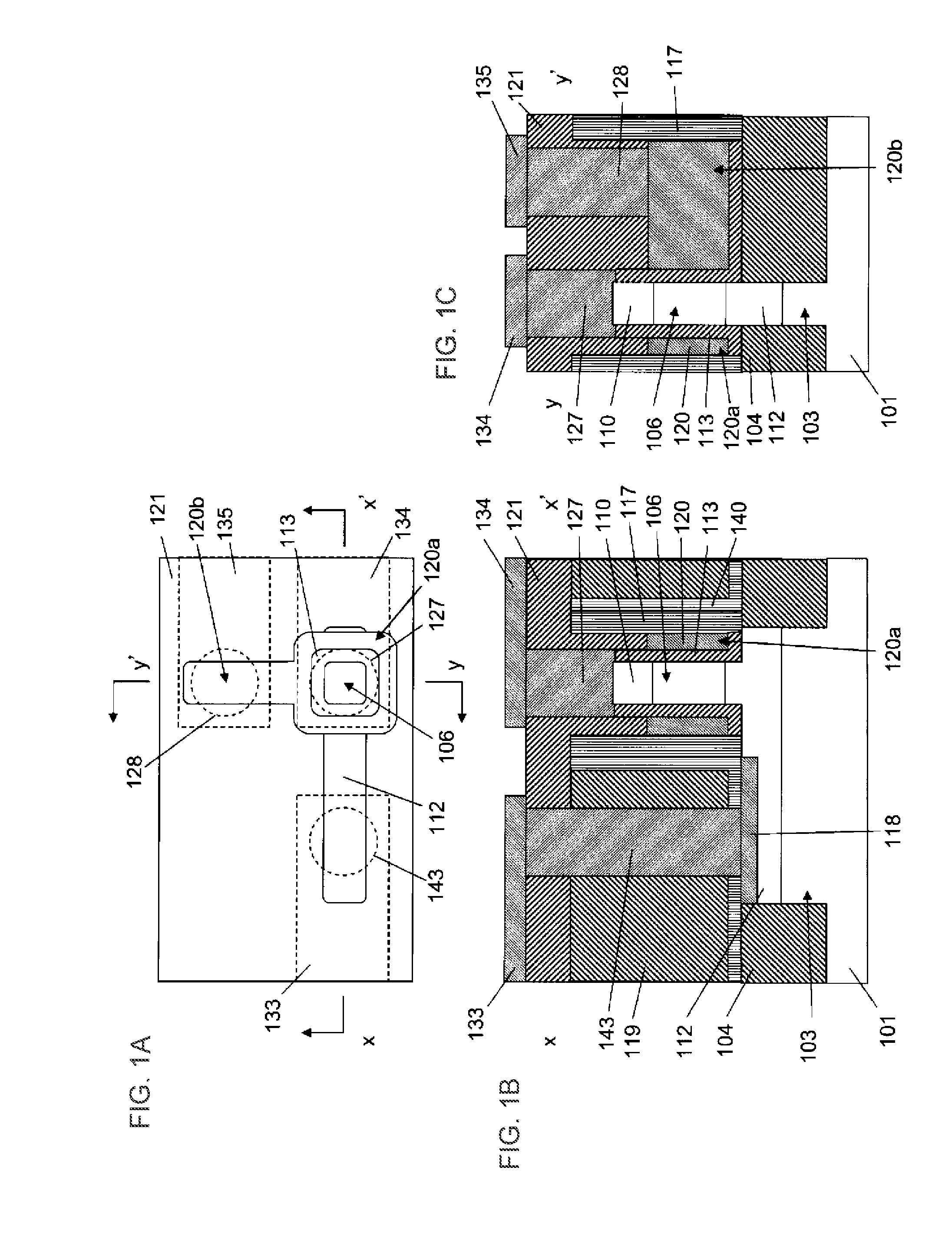
[0075]A manufacturing process for forming a SGT structure according to an embodiment of the present invention is described below with reference to FIGS. 2A-C to 42A-C.

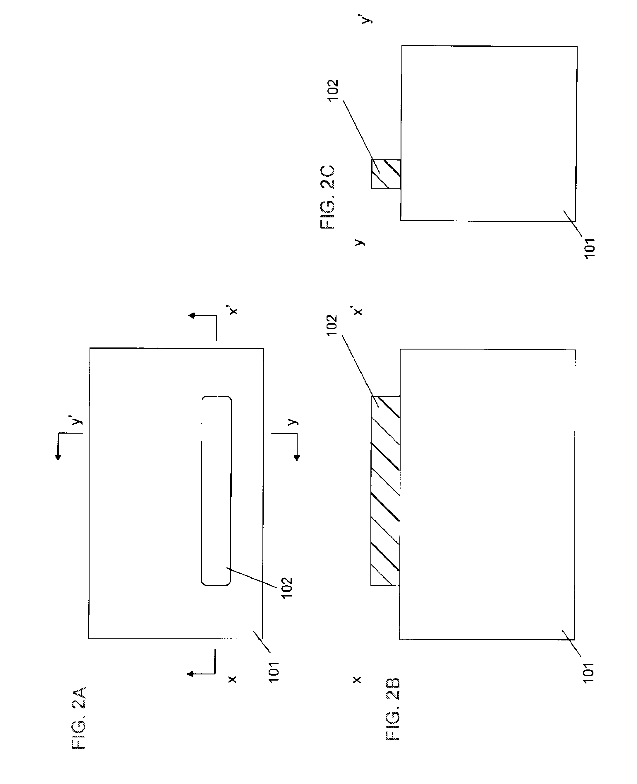
[0076]First, a manufacturing method for forming a fin-shaped semiconductor layer on a semiconductor substrate, forming a first insulating film around the fin-shaped semiconductor layer, and forming a pillar-shaped semiconductor layer on the fin-shaped semiconductor layer is described. As shown in FIG. 2, a first resist 102 is formed for forming a fin-shaped semiconductor layer on a semiconductor substrate 101.

[0077]As shown in FIGS. 3A-C, the semiconductor substrate 101 is etched to form a fin-shaped semiconductor layer 103. Although, in this case, the fin-shaped semiconductor layer is formed using the resist as a mask, a hard mask such as an oxide film or a nitride film may be used.

[0078]As shown in FIGS. 4A-C, the first resist 102 is removed.

[0079]As shown in FIGS. 5A-C, a first insulating film 104 is deposited aroun...


PUM


Abstract

A semiconductor device includes a fin-shaped semiconductor layer on a surface of a semiconductor substrate having a longitudinal axis extending in a first direction parallel to the surface. A first insulating film is around the fin-shaped semiconductor layer and a pillar-shaped semiconductor layer is on the fin-shaped semiconductor layer. A pillar diameter of the bottom of the pillar-shaped semiconductor layer is equal to a fin width of the top of the fin-shaped semiconductor layer, the pillar diameter and the fin width parallel to the surface. A gate insulating film is around the pillar-shaped semiconductor layer and a metal gate electrode is around the gate insulating film. A metal gate wiring is connected to the metal gate electrode and has a longitudinal axis extending in a second direction parallel to the surface and perpendicular to the first direction of the longitudinal axis of the fin-shaped semiconductor layer.

Description

RELATED APPLICATIONS[0001]This application is continuation-in-part application of U.S. patent application Ser. No. 14 / 061,082 filed Oct. 23, 2013, which is a divisional application of U.S. patent application Ser. No. 13 / 666,445 filed Nov. 1, 2012, which, pursuant to 35 U.S.C. §119(e), claims the benefit of U.S. Provisional Application No. 61 / 557,501 filed Nov. 9, 2011. The entire disclosures of which are incorporated by reference herein.BACKGROUND OF THE INVENTION[0002]1. Field of the Invention[0003]The present invention relates to a semiconductor device.[0004]2. Description of the Related Art[0005]Semiconductor integrated circuits, particularly integrated circuits using MOS transistors, are increasing in integration. With increases in integration, MOS transistors used in the integrated circuits are increasingly made finer up to a nano region. Finer MOS transistors have the problem of difficulty in suppressing leak currents and difficulty in decreasing the areas occupied by circuits...

Claims


Application Information

Patent Timeline
IPC IPC(8): H01L29/06H01L21/762H01L29/66H01L29/786H01L29/423
CPCH01L29/0653H01L29/78642H01L21/76224H01L29/42392H01L29/66666H01L29/78696H01L21/823431H01L21/823487H01L21/823821H01L21/823885H01L29/42372H01L29/4238H01L29/7827H01L29/66787
Inventor MASUOKA, FUJIONAKAMURA, HIROKI
Owner UNISANTIS ELECTRONICS SINGAPORE PTE LTD
Why Eureka
Try Eureka