Liquid crystal display device, manufacturing method thereof, and fabrication apparatus therefor

Inactive Publication Date: 2005-06-07
PANASONIC LIQUID CRYSTAL DISPLAY CO LTD +1
View PDF11 Cites 2 Cited by
  • Summary
  • Abstract
  • Description
  • Claims
  • Application Information

AI Technical Summary

Benefits of technology

[0041]An object of the present invention is to provide a liquid crystal display device capable of high-quality image display by solving the above problems in the art as well as a

Problems solved by technology

Particularly in liquid crystal display devices of the IPS scheme, there may occur what is called “spot contamination” that are

Method used


Image

  • Liquid crystal display device, manufacturing method thereof, and fabrication apparatus therefor
  • Liquid crystal display device, manufacturing method thereof, and fabrication apparatus therefor
  • Liquid crystal display device, manufacturing method thereof, and fabrication apparatus therefor

Examples


first embodiment

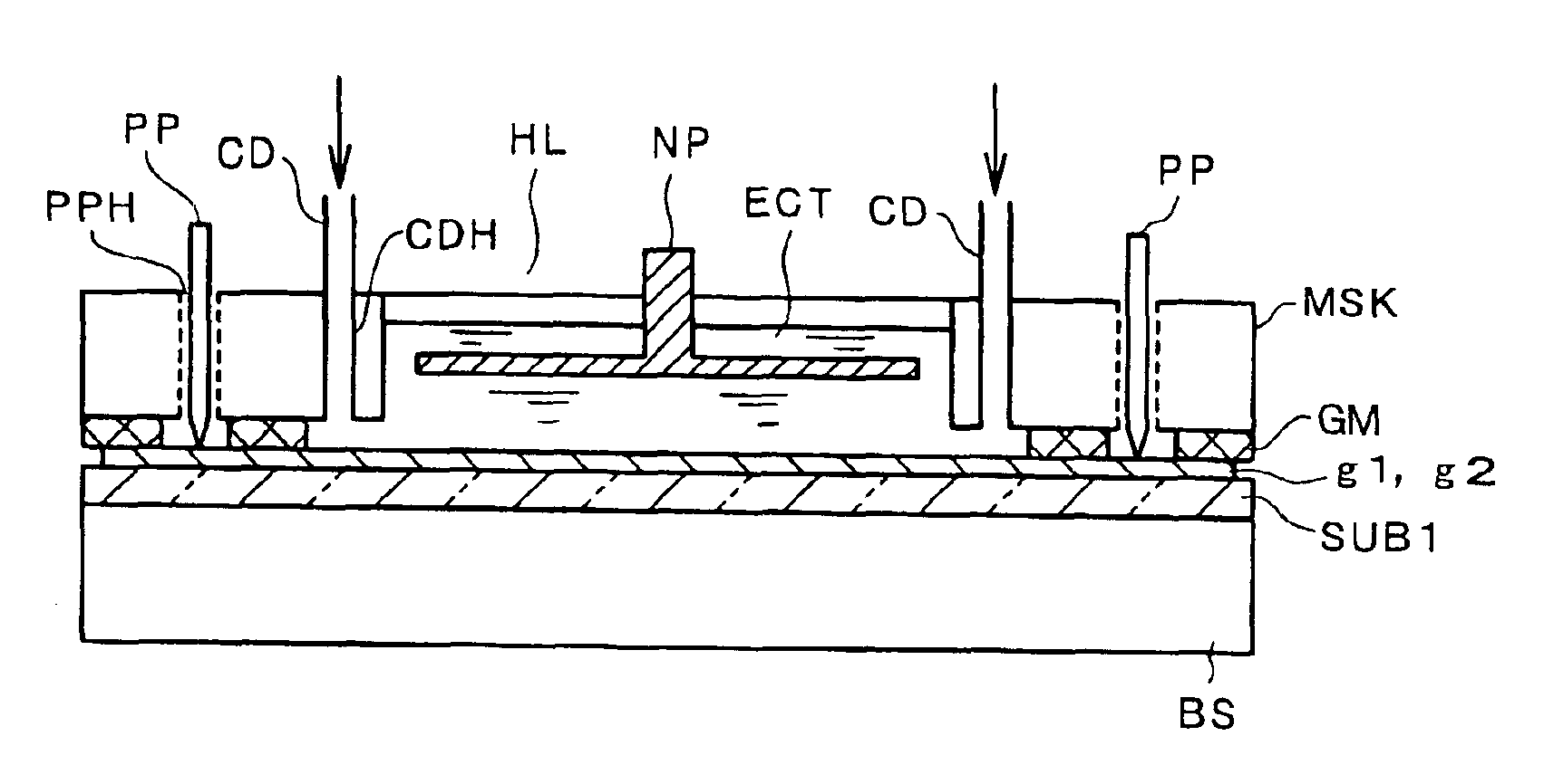
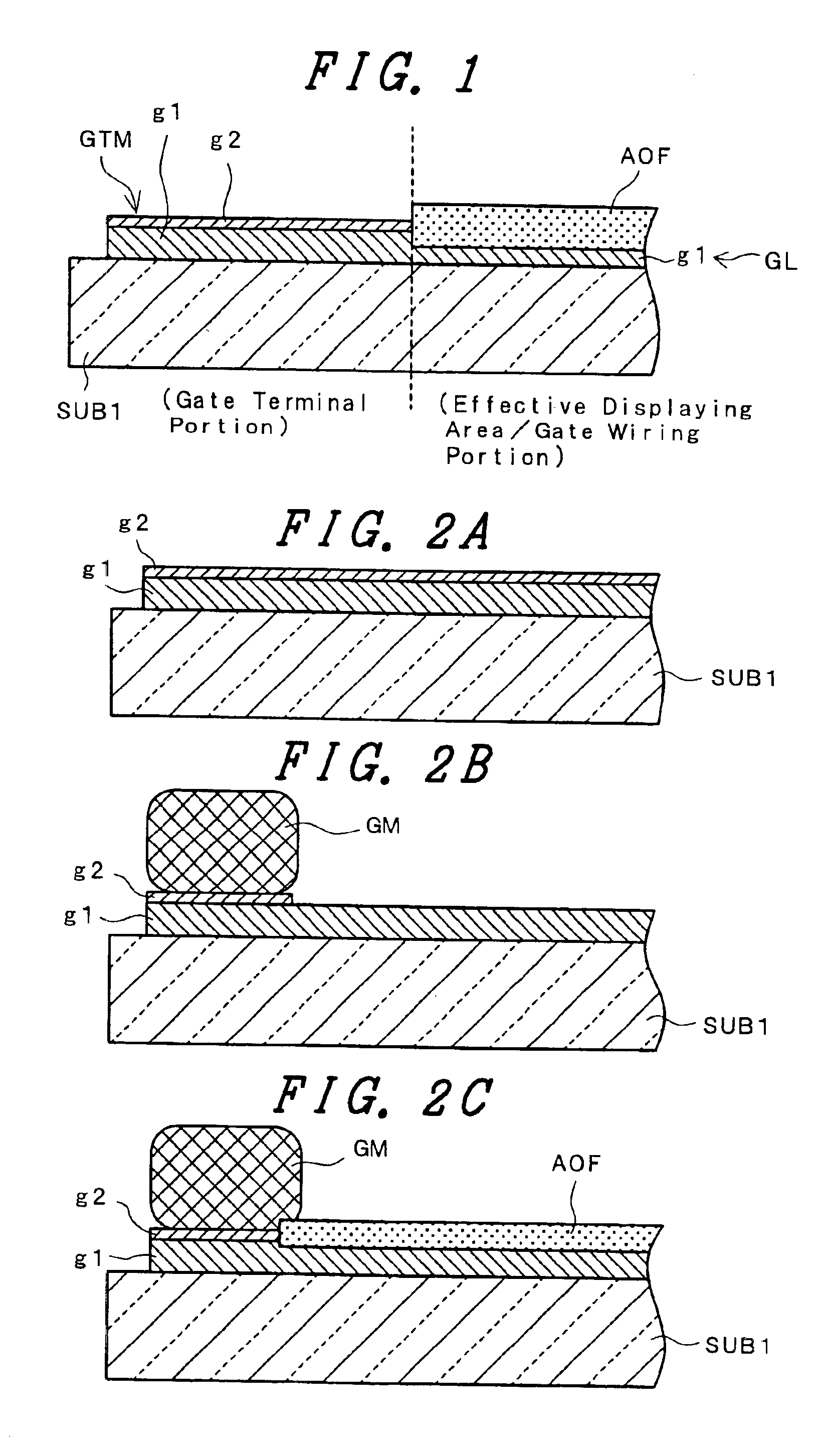
[0066]FIG. 1 is a sectional view of an important part of a thin-film transistor substrate according to the invention and schematically shows the structure of the thin-film transistor substrate. In FIG. 1, reference symbol SUB1 denotes a substrate called as the thin-film transistor substrate, and a transparent glass substrate is utilized therefor in this embodiment.

[0067]An effective displaying area / gate wiring portion in which a number of pixels as described above with reference to FIG. 17 are arranged and a gate terminal portion for leading out the gate lines in the gate wiring portion are formed on the substrate SUB1. In FIG. 1, the two portions are divided by a vertical broken line.

[0068]Each gate line GL in the effective displaying area (gate wiring portion) is formed by removing a top-layer molybdenum alloy thin film g2 from a lamination film of an aluminum alloy thin film g1 and the molybdenum alloy thin film g2 and then forming an aluminum anodic oxidation film AOF (aluminum ...

second embodiment

[0117]Although in the second embodiment the invention is applied to gate lines and gate terminals, the invention can also be applied to drain lines and drain terminals of the IPS scheme or the TN scheme and counter voltage signal lines and their terminals of the IPS scheme.

[0118]Also according to the second embodiment, the patterning of gate lines by electrolytic etching and the formation of aluminum oxide insulating layers can be performed continuously by using the same electrolytic etching liquid. Therefore, the occurrence of display defects such as spot contaminations can be prevented by the insulating layers and the manufacturing cost can be reduced because the number of manufacturing steps does not increase.

[0119]When the first and second embodiments are applied to actual manufacture of a liquid crystal display device, a 30% reduction in manufacturing cost was attained. Further, the employment of aluminum-oxide-coated aluminum lines increased the yield factor by about 10%.

[0120...


PUM

PropertyMeasurementUnit
Electric potential / voltageaaaaaaaaaa

Abstract

A method of manufacturing an LCD device which includes a gate line having an effective display area which includes an aluminum alloy layer and an aluminum oxide layer. The gate line also includes a gate terminal portion which is made up of the same aluminum alloy layer with a molybdenum alloy layer formed thereon. To form this structure, an insulating substrate of the LCD device, with the laminated structure of the aluminum alloy layer and the molybdenum layer, is immersed in an electrolytic solution. During the immersion, the molybdenum layer is etched off the aluminum alloy in the effective displaying area, while the etching is prevented in the gate terminal area by a protective layer. Following this, the aluminum oxide layer is formed over the aluminum alloy in the effected display area while the device is still immersed in the electrolytic solution.

Description

CROSS-REFERENCE TO RELATED APPLICATIONS[0001]This application is a Divisional application of Application Ser. No. 09 / 951,425, filed Sep. 14, 2001 now abandoned, the entire disclosure of which is hereby incorporated by reference.BACKGROUND OF THE INVENTION[0002]1. Field of the Invention[0003]The present invention is related to a liquid crystal display device, particularly to a liquid crystal display device disposing a pair of insulating substrates opposite to one another with a predetermined gap by interposing spacers therebetween, holding liquid crystal compounds, and having an additional capacitance portion formed in a pixel area, a manufacturing method of the liquid crystal display device, and a fabrication apparatus for the liquid crystal display device.[0004]2. Description of the Related Art[0005]High-resolution liquid crystal display devices capable of color display for notebook-sized computers and computer monitors are spread widely.[0006]Those liquid crystal display devices a...

Claims


Application Information

Patent Timeline
IPC IPC(8): G02F1/13G02F1/1362G02F1/1343G02F1/136C23C28/02C25F3/02G02F1/1368G09F9/30H01L21/3063H01L21/336H01L29/786
CPCG02F1/136286G02F1/13458G02F1/134363G02F2001/13629G02F1/13629G02F1/136
Inventor TAKAHASHI, TOMOAKIKANEKU, SAKARIYAMAMOTO, HIDEAKINAKATANI, MITSUOSASAKI, HIROSHI
Owner PANASONIC LIQUID CRYSTAL DISPLAY CO LTD
Why Eureka
Try Eureka