Semiconductor device and manufacturing method thereof

a technology of semiconductors and semiconductors, applied in semiconductor devices, electrical devices, transistors, etc., can solve the problems of increasing manufacturing costs, limited usable substrates, and substrate shrinkage by high-temperature heat treatment, and achieves high current, reduced sheet resistance, and high current

Inactive Publication Date: 2007-06-07
SEMICON ENERGY LAB CO LTD
View PDF9 Cites 16 Cited by
  • Summary
  • Abstract
  • Description
  • Claims
  • Application Information

AI Technical Summary

Benefits of technology

[0018] In accordance with the present invention, a semiconductor device with a high ON current can be obtained by controlling the shape of a silicide layer. In addition, a semiconductor device with a high ON current can be obtained with reduced sheet resistance. Further, an ON current can be heightened without increasing the number of manufacturing steps of a semiconductor device. Accordingly, a high ON current can be obtained with a maintained manufacturing cost of a conventional semiconductor device. In addition, since high-temperature heat treatment is not required to obtain a high ON current, a substrate with low heat resistance can also be used; accordingly, a substrate can be employed without the limitation on heat resistance.

Problems solved by technology

However, in these methods, one heat treatment step is added, and an apparatus for the heat treatment is additionally required; accordingly, there has been a problem in increasing manufacturing cost.
In addition, in the case where a substrate with low heat resistance such as a glass substrate is used as a substrate, the substrate might be shrunk by the high-temperature heat treatment.
Therefore, usable substrates have been limited to a substrate with high heat resistance, and there has been a problem of reducing the selection freedom of the substrate.

Method used


Image

  • Semiconductor device and manufacturing method thereof
  • Semiconductor device and manufacturing method thereof
  • Semiconductor device and manufacturing method thereof

Examples


embodiment mode 1

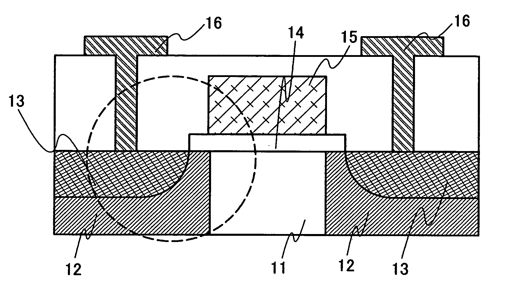
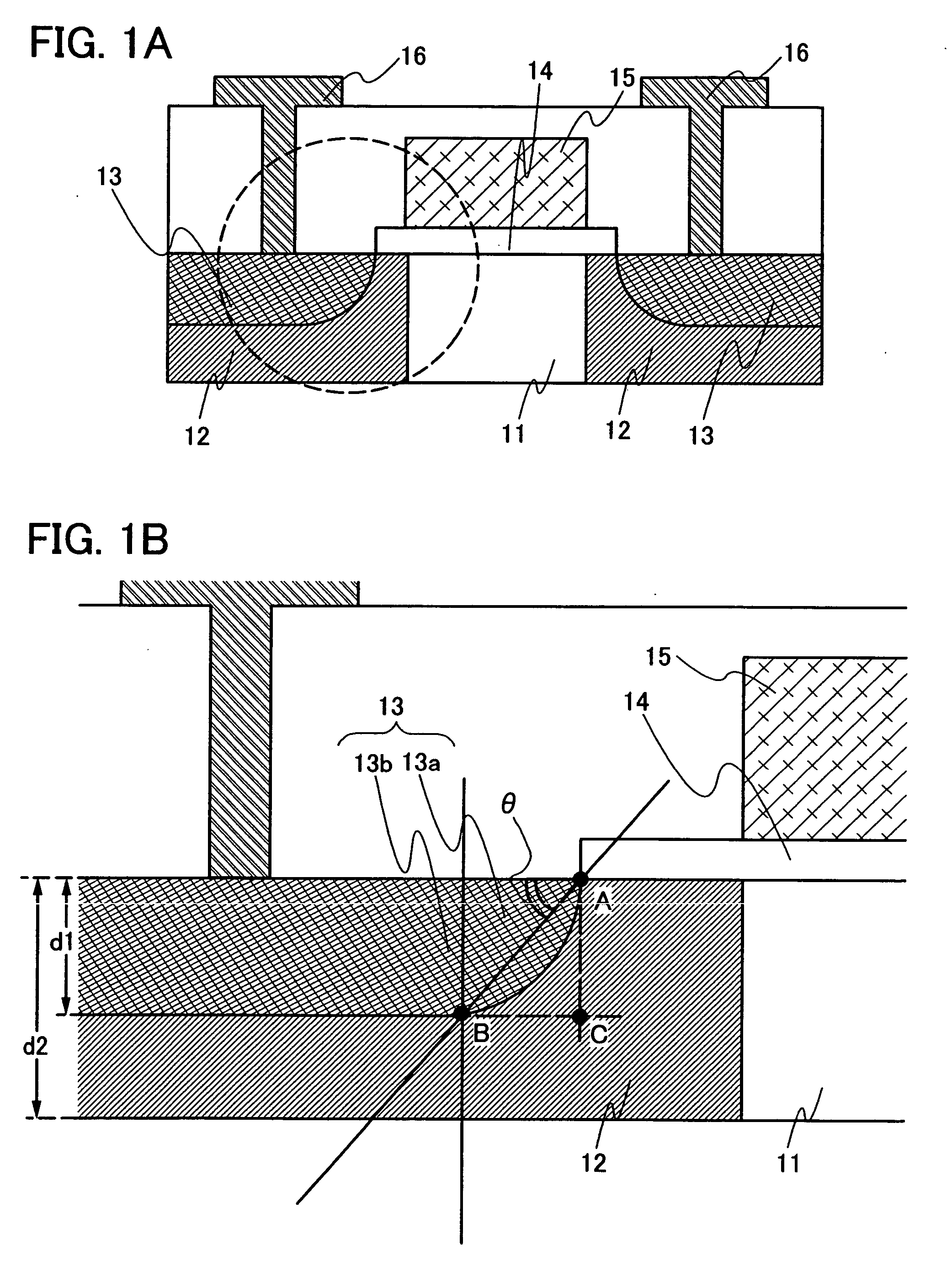
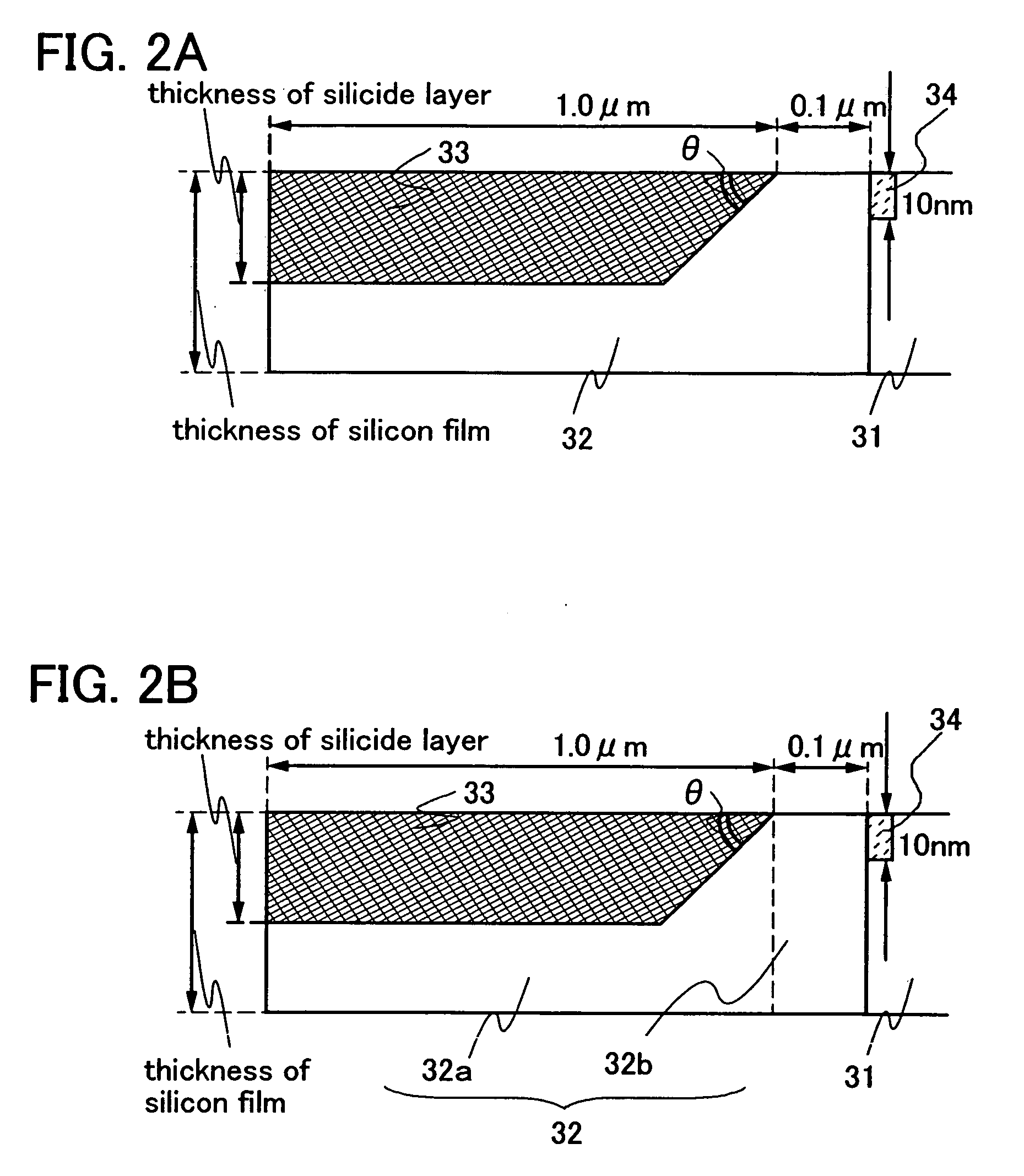
[0052] In the present invention, it was analyzed that how the thickness and shape of silicide affected on an ON current in a transistor including a silicide layer.

[0053]FIGS. 2A and 2B are schematic views showing a part of a silicon film which is a semiconductor film of a top-gate transistor, and also showing a structure of an element assumed in this analysis. FIGS. 2A and 2B schematically show the part of the silicon film surrounded by a dashed line of FIG. 1A. The element used in the analysis may be any of a thin film transistor (TFT), a transistor formed directly over a silicon substrate, and a transistor formed over a silicon-on-insulator (SOI) substrate such as a separation by implanted oxygen (SIMOX) substrate.

[0054]FIG. 2A shows an element structure in the case where a low-concentration impurity region does not exist between a silicide layer 33 and a region 31. FIG. 2B shows an element structure in the case where a low-concentration impurity region exists between the silici...

embodiment mode 2

[0085] A manufacturing method of a semiconductor device of the present invention will be described with reference to FIGS. 16A to 18B.

[0086] First, an insulating film 102 is formed with a thickness of 100 to 300 nm over a substrate 101. As the substrate 101, an insulating substrate such as a glass substrate, a quartz substrate, a plastic substrate or a ceramic substrate, a metal substrate, or the like can be used.

[0087] As the insulating film 102, a single-layer structure having an insulating film including oxygen or nitrogen such as silicon oxide (SiOx), silicon nitride (SiNx), silicon oxide including nitrogen (SiOxNy) (x>y) (also referred to as silicon oxynitride), or silicon nitride including oxygen (SiNxOy) (x>y) (also referred to as silicon nitride oxide), or a stack structure including the above-described film can be used. Although the insulating film 102 is not necessarily provided, the insulating film 102 is preferably formed in the case where contamination from the substr...

embodiment mode 3

[0124] A manufacturing method of a semiconductor device including a low-concentration impurity region will be described with reference to FIGS. 19A to 20F. The same reference numerals are commonly given to the same components or components having the same function as those in Embodiment Mode 2, and the detailed explanation thereof will be omitted.

[0125] First, the process until the structure of FIG. 19A has been formed is the same as the process until the structure of FIG. 16A in Embodiment Mode 2 has been formed. Then, doping with an impurity ion 201 at a low concentration is conducted (FIG. 19B). The impurity ion 201 passes through the gate insulating film 104 to dope the island-like semiconductor film 103, to form low-concentration impurity regions 202 and 203 and a channel formation region 109. As a doping method, an ion doping method or an ion implantation method can be employed. For example, in the case of manufacturing a P-type semiconductor, boron (B), gallium (Ga), or the ...


PUM


Abstract

It is an object of the present invention to obtain a transistor with a high ON current including a silicide layer without increasing the number of steps. A semiconductor device comprising the transistor includes a first region in which a thickness is increased from an edge on a channel formation region side and a second region in which a thickness is more uniform than that of the first region. The first and second region are separated by a line which is perpendicular to a horizontal line and passes through a point where a line, which passes through the edge of the silicide layer and forms an angle θ (0° <θ<45°) with the horizontal line, intersects with an interface between the silicide layer and an impurity region, and the thickness of the second region to a thickness of a silicon film is 0.6 or more.

Description

BACKGROUND OF THE INVENTION [0001] 1. Field of the Invention [0002] The present invention relates to a semiconductor device including a silicide layer and a manufacturing method thereof. [0003] 2. Description of the Related Art [0004] In accordance with the reduction of an integrated circuit, a semiconductor device which forms an integrated circuit is required to have a lower contact resistance with a metal wiring and a lower resistance of an impurity region. Therefore, a technique in which a contact resistance or a resistance of an impurity region is reduced by forming a silicide layer in a semiconductor film is adopted in a semiconductor field (for example, Patent Document 1: Japanese Published Patent Application No. 2004-221115). When a resistance of a semiconductor film is reduced, an ON current of a semiconductor device is improved and a semiconductor device with a high characteristic can be manufactured. [0005] On the other hand, when a silicide layer of a semiconductor is thi...

Claims


Application Information

Patent Timeline
Patent Type & Authority Applications(United States)
IPC IPC(8): H01L29/76
CPCH01L21/84H01L27/1203H01L29/458H01L29/665H01L29/66636H01L29/78618H01L2924/01004H01L2924/01012H01L2924/01029H01L2924/01078H01L2924/01079H01L2924/04941H01L2924/15184H01L2924/15311H01L2924/19041H01L2924/01067H01L2224/16225H01L2224/32225H01L2224/48227H01L2224/73265H01L2924/01068H01L2224/45144H01L2924/00H01L2924/13091H01L2924/00012H01L2924/3025H01L2924/12044H01L24/73H01L2924/14
Inventor GODO, HIROMICHITOKUNAGA, HAJIME
Owner SEMICON ENERGY LAB CO LTD
Why Eureka
Try Eureka