Method for forming pattern, method for manufacturing light emitting device, and light emitting device

a technology of light emitting devices and manufacturing methods, which is applied in the direction of solid-state devices, electric lighting sources, electric light sources, etc., can solve the problems of degrading the electric characteristics of light emitting elements and increasing the number of manufacturing steps, and achieves easy forming, high accuracy, and increased manufacturing steps

Active Publication Date: 2009-01-08
SEMICON ENERGY LAB CO LTD
View PDF14 Cites 38 Cited by
  • Summary
  • Abstract
  • Description
  • Claims
  • Application Information

AI Technical Summary

Benefits of technology

[0024]According to the present invention, a pattern can be formed easily with high accuracy without using a specific metal mask and increasing the number of manufacturing steps by forming a liquid-repellent part and a lyophilic part as selected on a surface where a film is to be formed. Thus, loss of a material can be reduced. In addition, since a metal mask or a photolithography process for forming a pattern is not necessary, the process can be simplified, and the low cost can be achieved.

Problems solved by technology

However, these methods have problems in that a specific metal mask is necessary so that light irradiation is partially performed, and the number of manufacturing steps is increased since a photolithography technique is used for irradiation in pattern.
Further, in the latter example, there are also problems in that when the amount of the binder is increased to smooth the layer containing a photocatalyst, constituents of the binder with an insulating property remain on the electrode which is modified to be lyophilic, and electric characteristics of the light emitting element are degraded.

Method used


Image

  • Method for forming pattern, method for manufacturing light emitting device, and light emitting device
  • Method for forming pattern, method for manufacturing light emitting device, and light emitting device
  • Method for forming pattern, method for manufacturing light emitting device, and light emitting device

Examples


embodiment mode 1

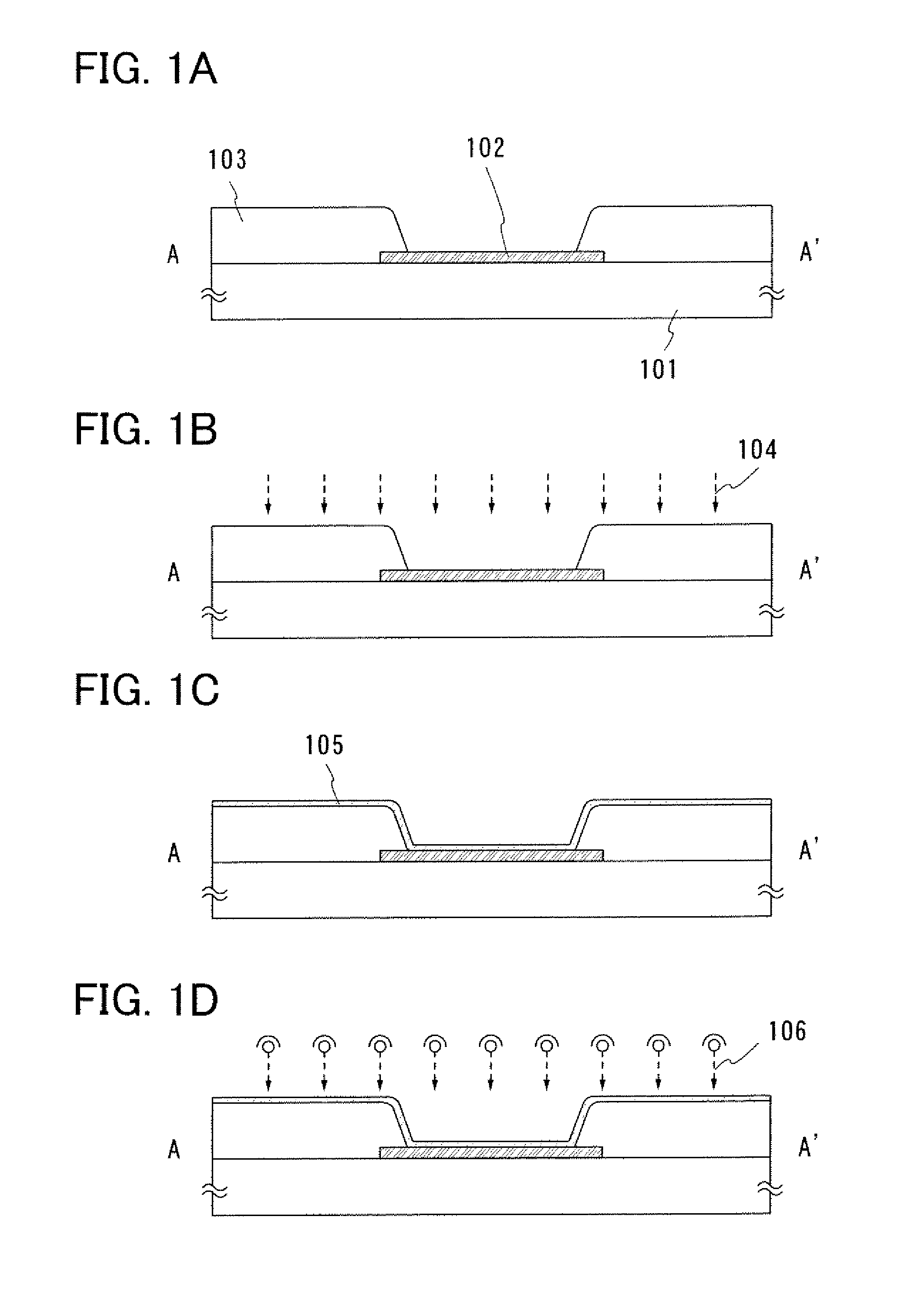
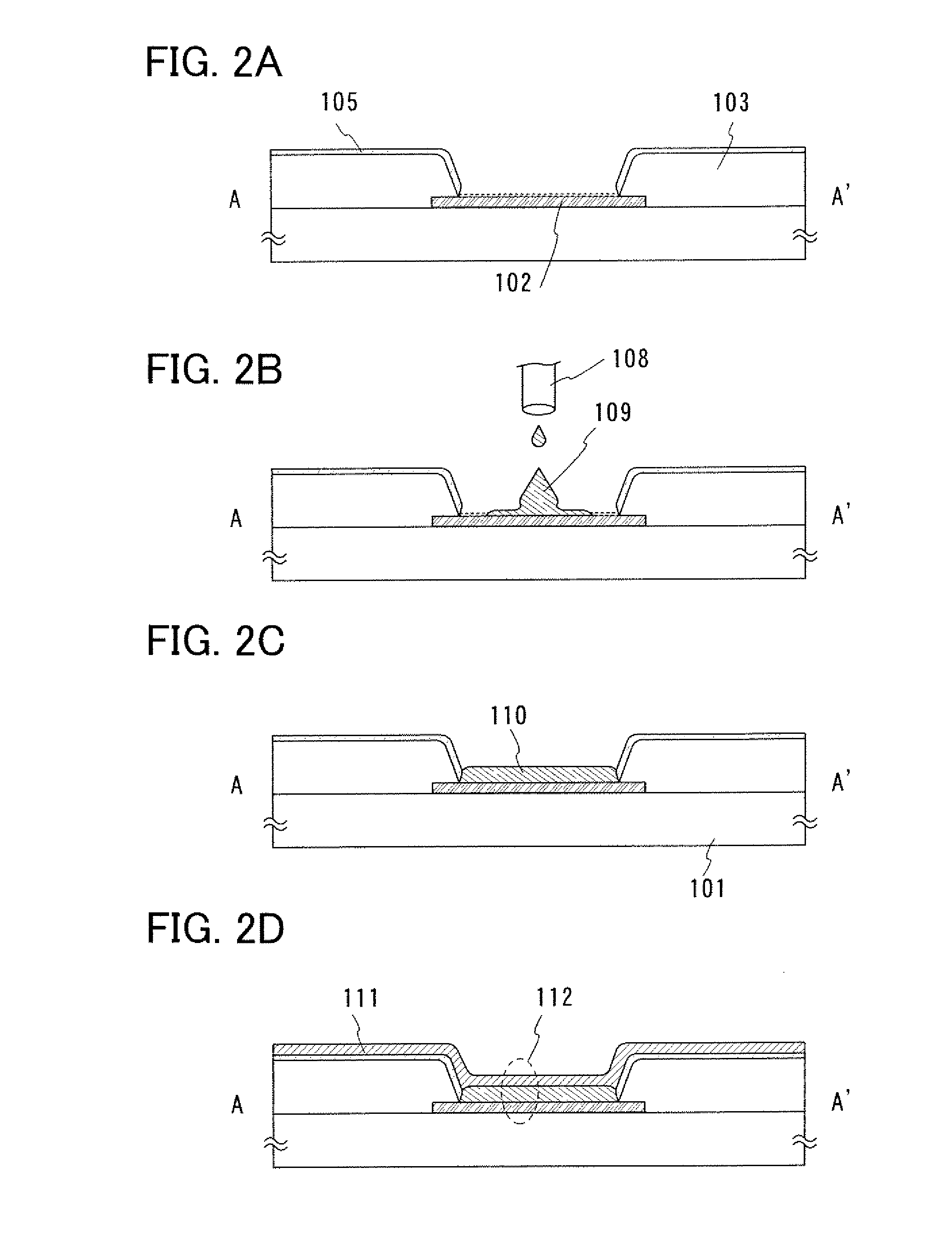
[0040]Embodiment Mode 1 will describe, as a method for forming a pattern of the present invention, a method for manufacturing a light emitting element in which a liquid-repellent part and a lyophilic part are separately formed over the surface of a substrate.

[0041]A photocatalytic conductive film 102 is formed over a substrate 101 as shown in FIG. 1A. Note that the photocatalytic conductive film 102 functions as one of electrodes of a light emitting element which is formed later.

[0042]For the substrate 101, a glass substrate, a quartz substrate, a substrate formed of an insulating substance such as ceramics, e.g., alumina, a plastic substrate, a silicon wafer, a metal plate, or the like can be used. In addition, for the photocatalytic conductive film 102, indium tin oxide (ITO), indium zinc oxide (IZO) which is obtained by mixing zinc oxide (ZnO) of 2% to 20% inclusive into indium oxide, indium tin oxide containing silicon oxide as a constituent, indium oxide doped with tin, zinc ox...

embodiment mode 2

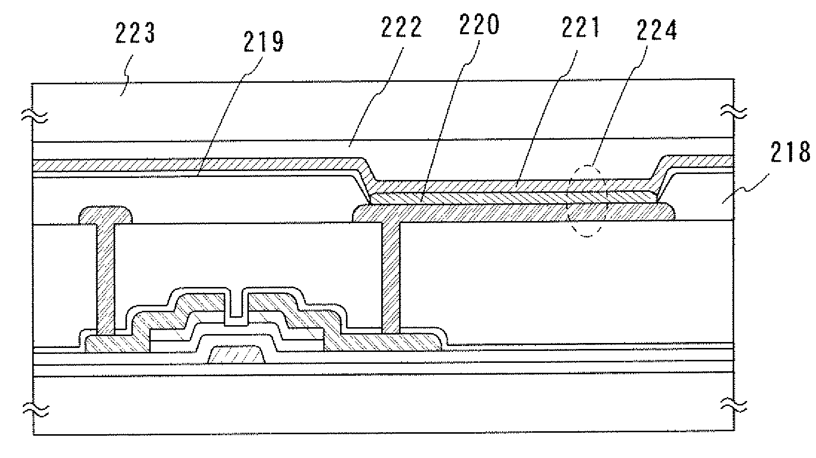
[0087]Embodiment Mode 2 will describe a method for manufacturing a light emitting device including a thin film transistor which is electrically connected to the light emitting element manufactured in Embodiment Mode 1, with reference to FIGS. 3A to 3D.

[0088]As shown in FIG. 3A, an insulating film 201 is formed over a substrate 200. The insulating film 201 functions as a base insulating film and suppresses mixture of impurity elements from a glass substrate into a semiconductor film which is formed later. The insulating film 201 is formed as needed. The insulating film 201 can be formed using an inorganic material such as silicon nitride oxide (SiNxOy (X>Y)), aluminum oxide, aluminum nitride, aluminum oxynitride, or aluminum nitride oxide.

[0089]As a specific example of the insulating film 201, a single layer structure of a silicon nitride film or a silicon oxynitride film with a thickness of less than or equal to 10 nm, or a two-layer structure in which a silicon nitride oxide film i...

embodiment mode 3

[0116]Embodiment Mode 3 will describe a method for manufacturing a light emitting device including a light emitting element electrically connected to an organic thin film transistor with reference to FIGS. 4A to 4D.

[0117]As in Embodiment Mode 2, an insulating film 301 is formed over a substrate 300. Then, a first conductive film 302 which functions as a gate electrode is formed over the insulating film 301. It is acceptable as long as the first conductive film 302 is formed of a metal which has an insulating property by nitridation or oxidation, preferably, tantalum (Ta), niobium (Nb), aluminum (Al), copper (Cu), titanium (Ti), or the like. Besides, tungsten (W), chromium (Cr), nickel (Ni), cobalt (Co), magnesium (Mg), or the like can also be used.

[0118]A manufacturing method of the first conductive film 302 is not limited to a particular method, and the first conductive film 302 may be formed by a sputtering method, an evaporation method, or the like and patterned into a desired sh...


PUM

PropertyMeasurementUnit
contact angleaaaaaaaaaa
wavelengthaaaaaaaaaa

Abstract

Oxidation treatment is performed to the surface of a substrate provided with a photocatalytic conductive film and an insulating film; treatment with a silane coupling agent is performed, so that a silane coupling agent film is formed and the surface of the substrate is modified to be liquid-repellent; and the surface of the substrate is irradiated with light of a wavelength (less than to equal to 390 nm) which has energy of greater than or equal to a band gap of a material for forming the photocatalytic conductive film, so that only the silane coupling agent film over the surface of the photocatalytic conductive film is decomposed and the surface of the photocatalytic conductive film can be modified to be lyophilic.

Description

BACKGROUND OF THE INVENTION[0001]1. Field of the Invention[0002]The present invention relates to a method for forming a pattern capable of forming a film as selected by controlling wettability of a surface where the film is to be formed, a method for manufacturing a light emitting device having a light emitting element using the method for forming a pattern, and a light emitting device.[0003]A light emitting element is an element having a structure in which a film containing an organic compound (hereinafter referred to as a layer containing an organic compound) is provided between a pair of electrodes, and fluorescence or phosphorescence can be obtained by application of an electric field.[0004]The light emitting device refers to an image display device, a light emitting device, or a light source (including a lighting device). Further, the light emitting device includes any of the following modules in its category: a module in which a connector such as a flexible printed circuit (FP...

Claims


Application Information

Patent Timeline
Patent Type & Authority Applications(United States)
IPC IPC(8): H01L21/283H01L33/00H01L51/50H05B33/10H05B33/22
CPCH01L21/76825H01L21/76826H01L27/3246H01L51/56H01L51/0005H01L51/0545H01L27/3283Y02P80/30H10K59/122H10K59/173H10K71/135H10K10/466H10K71/00
Inventor FUJII, GENTAKAHASHI, ERIKA
Owner SEMICON ENERGY LAB CO LTD
Why Eureka
Try Eureka