Infrared emitter

a technology of infrared light and emitter, which is applied in the direction of semiconductor devices, lamp incadescent bodies, electrical equipment, etc., can solve the problems of poor conversion of electrical energy into useful infrared radiation, difficult and costly fabrication of implementations using metals (woodpiles), and difficult to obtain a well-defined emission spectrum centered on a chosen central infrared wavelength. , to achieve the effect of enhancing the emitted infrared light intensity

Active Publication Date: 2016-11-24
CSEM CENT SUISSE DELECTRONIQUE & DE MICROTECHNIQUE SA RECH & DEV
View PDF0 Cites 7 Cited by
  • Summary
  • Abstract
  • Description
  • Claims
  • Application Information

AI Technical Summary

Benefits of technology

[0030]In an embodiment the reflecting layer is arranged to focus at least a portion of the reflected por

Problems solved by technology

The limiting issues with these infrared light sources are mainly:their infrared emission spectrum follows closely the one of a blackbody;the emitted radiation is omnidirectional, such as a Lambertian angular distribution;the light modulation is very limited and intensity modulation frequencies are typically smaller than some Hertz;the conversion of the electrical energy in useful infrared radiation is poor;the packaging of these light source requires often a vacuum or inert gas environment.
The implementations using metals (woodpiles) are extremely difficult and costly to fabricate.
Variants based on dielectrics, while showing a non-blackb

Method used


Image

  • Infrared emitter
  • Infrared emitter
  • Infrared emitter

Examples


Embodiment Construction

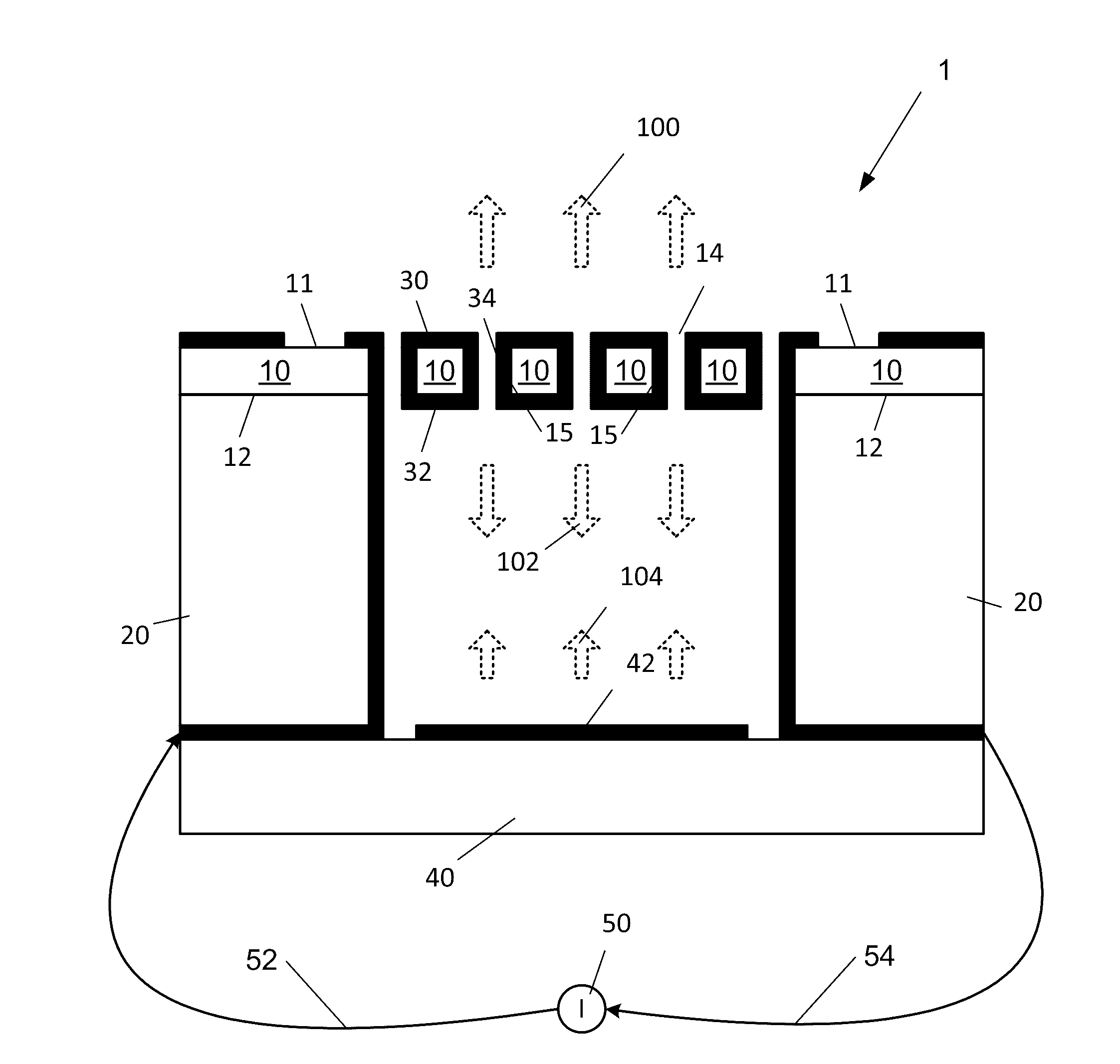
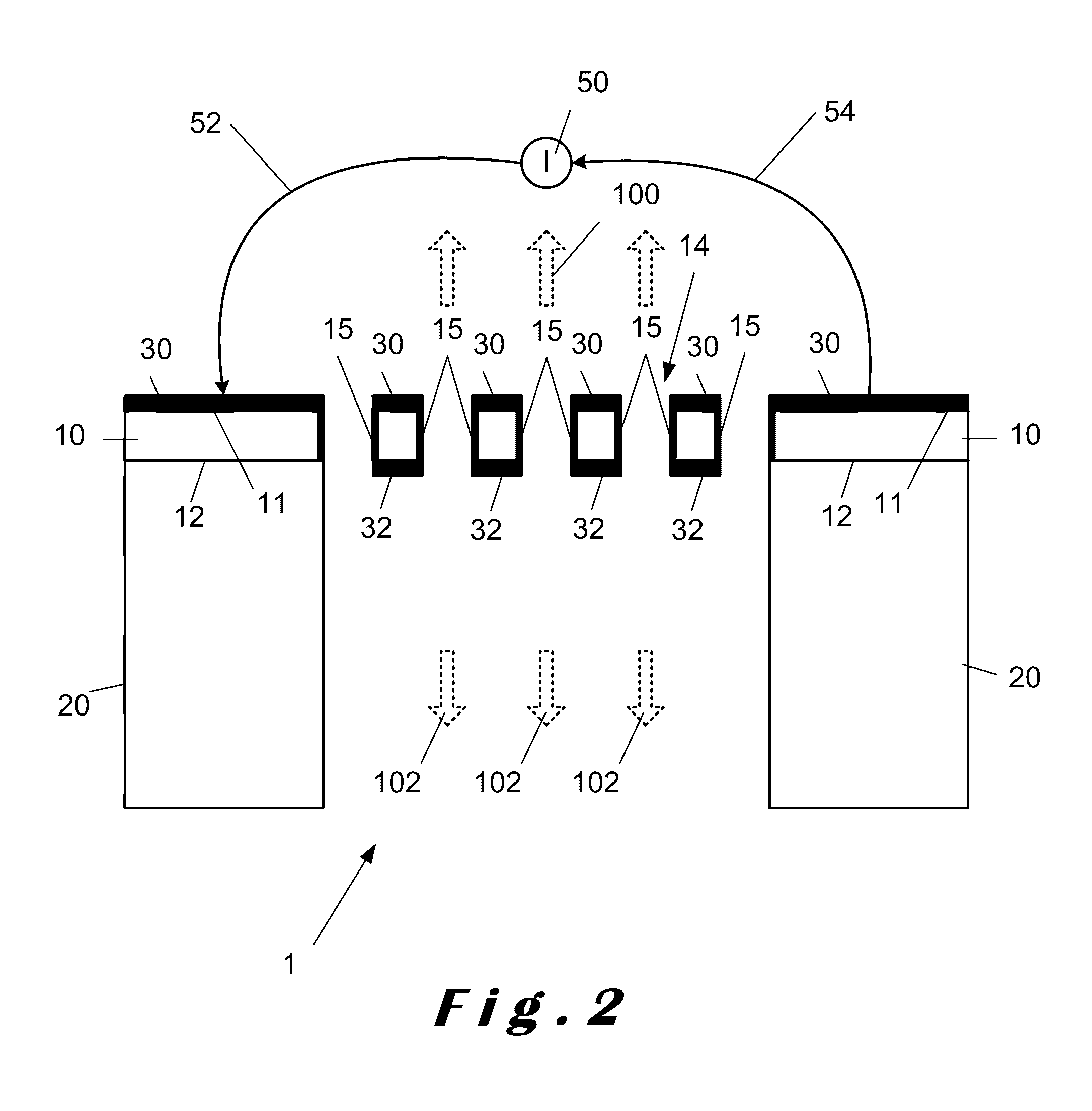
[0046]A representative embodiment of the infrared light emitter according to the disclosure is illustrated in FIG. 2. A substantially flat membrane 10, illustrated in FIG. 3, comprises a first surface 11 and a second surface 12 substantially parallel to the first surface 11. The flat membrane 10 comprises an array 13 of infrared wavelength sized through-holes 14. A first metal layer 30 is arranged on the first surface 11 and a second metal layer 32 is arranged on the second surface 12. The first metal layer 30 and the second 32 metal layer are deposited on the membrane 10 by conventional metal deposition techniques but other techniques may be used as well. A typical thickness of the metal layers 30, 32 is 0.5 μm. Preferably the thickness of the metal layers 30, 32 is more than 100 nm in order to assure a continuous and well adherent metal layer on the membrane, but thicknesses of less than 100 nm may be devised also for other applications, such as those requiring high modulation fre...


PUM


Abstract

The disclosure concerns an infrared emitter is provided comprising a metalized membrane emitting infrared light in operation. The membrane comprises a two dimensional array of infrared wavelength sized through-holes and to each side a thin metal layer comprising also an array of through-holes. The through-holes are arranged as a two-dimensional periodic array and each of said through-holes have a cross section having a maximum and a minimum dimension of less than any wavelength of the emitted infrared light. The peak wavelength of the emitted infrared light is proportional to the periodicity of the through-holes. At least one of the metal layers is connected to an electrical current source that provides an electrical current that heats at least one of the metal layers so that a narrow bandwidth and highly directive light beam of infrared light is emitted. The membrane is arranged on a membrane support and both are made of a material that resists to temperatures higher than 400°.

Description

FIELD OF THE DISCLOSURE[0001]The present disclosure relates to the field of infrared light emitting devices. More particularly, the present disclosure relates to a micro-machined narrow-band infrared light emitter having a directional light emission and which is based on a membrane comprising an array of holes.BACKGROUND[0002]Despite the wide diversity of available infrared light sources, there is no equivalent in the infrared of a light emitting device (LED), i.e. an intense light source having a limited infrared spectral linewidth, a good directivity of its emitted infrared light beam and which is easy to manufacture, so relatively cheap.[0003]Instead, there are a great variety of thermal light sources which are used for low end applications. The limiting issues with these infrared light sources are mainly:[0004]their infrared emission spectrum follows closely the one of a blackbody;[0005]the emitted radiation is omnidirectional, such as a Lambertian angular distribution;[0006]the...

Claims


Application Information

Patent Timeline
IPC IPC(8): H01L33/60H01L33/26H01L33/58H01L33/62H01L33/48
CPCH01L33/60H01L33/62H01L2933/0091H01L33/58H01L33/26H01L33/483H01K1/04H01K1/14H01L27/153
Inventor STANLEY, ROSSTIMOTIJEVIC, BRANISLAV
Owner CSEM CENT SUISSE DELECTRONIQUE & DE MICROTECHNIQUE SA RECH & DEV
Why Eureka
Try Eureka