Fingerprint sensing device with heterogeneous coating structure comprising a mold

Active Publication Date: 2016-12-08
FINGERPRINT CARDS ANACATUM IP AB
View PDF22 Cites 16 Cited by
  • Summary
  • Abstract
  • Description
  • Claims
  • Application Information

AI Technical Summary

Benefits of technology

[0027]According to one embodiment of the invention, the coating material may advantageously be a photoresist. By using a photoresist, the cavities can be formed using conventional photolithography and development processes, which simplifies the overall process flow. Moreover, a photoresist can easily be tailored to have a specific dielectric constant so that a desired ratio of dielectric constants can be achieved. Furthermore, a photoresist can be deposited on a full wafer with a high degree of accuracy and thickness uniformity, using for example spin coating or spray coating.
[0028]In one embodiment of the invention the, the method may further comprise plasma cleaning of the coating material prior to the step of providing the mold material. The plasma cleaning of the surface of the coating material improves the wetting of the coating which in turn improves the filling of the cavities by the mold material. Plasma cleaning also provides a surface with improved adhesion to the mold material.
[0029]According to one embodiment of the invention, the method may further comprise depositing an adhesive on the mold material; and attaching a

Problems solved by technology

This in turn leads to an image blurring effect.
As a function of an increased distance between a finger and any given pixel, each pixel is starting to receive signals from areas that are not immediately located vertically on top of said pixel resulting in image blurring negatively impacting the capabilities of the sensors to resolve fine features in a fingerprint.
However, a direct electrical contact between the finger and the pixel may cause problems related to elec

Method used


Image

  • Fingerprint sensing device with heterogeneous coating structure comprising a mold
  • Fingerprint sensing device with heterogeneous coating structure comprising a mold
  • Fingerprint sensing device with heterogeneous coating structure comprising a mold

Examples


Embodiment Construction

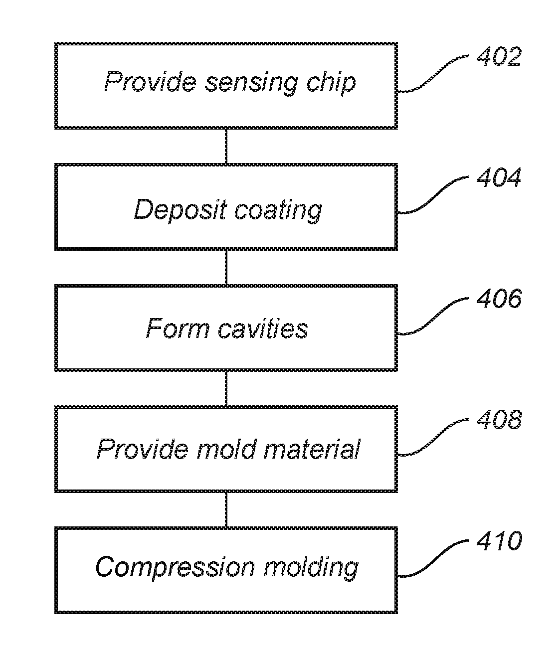
[0050]In the present detailed description, various embodiments of a fingerprint sensing device according to the present invention are mainly discussed with reference to a capacitive fingerprint sensing device. A method for manufacturing a fingerprint sensing device is also discussed.

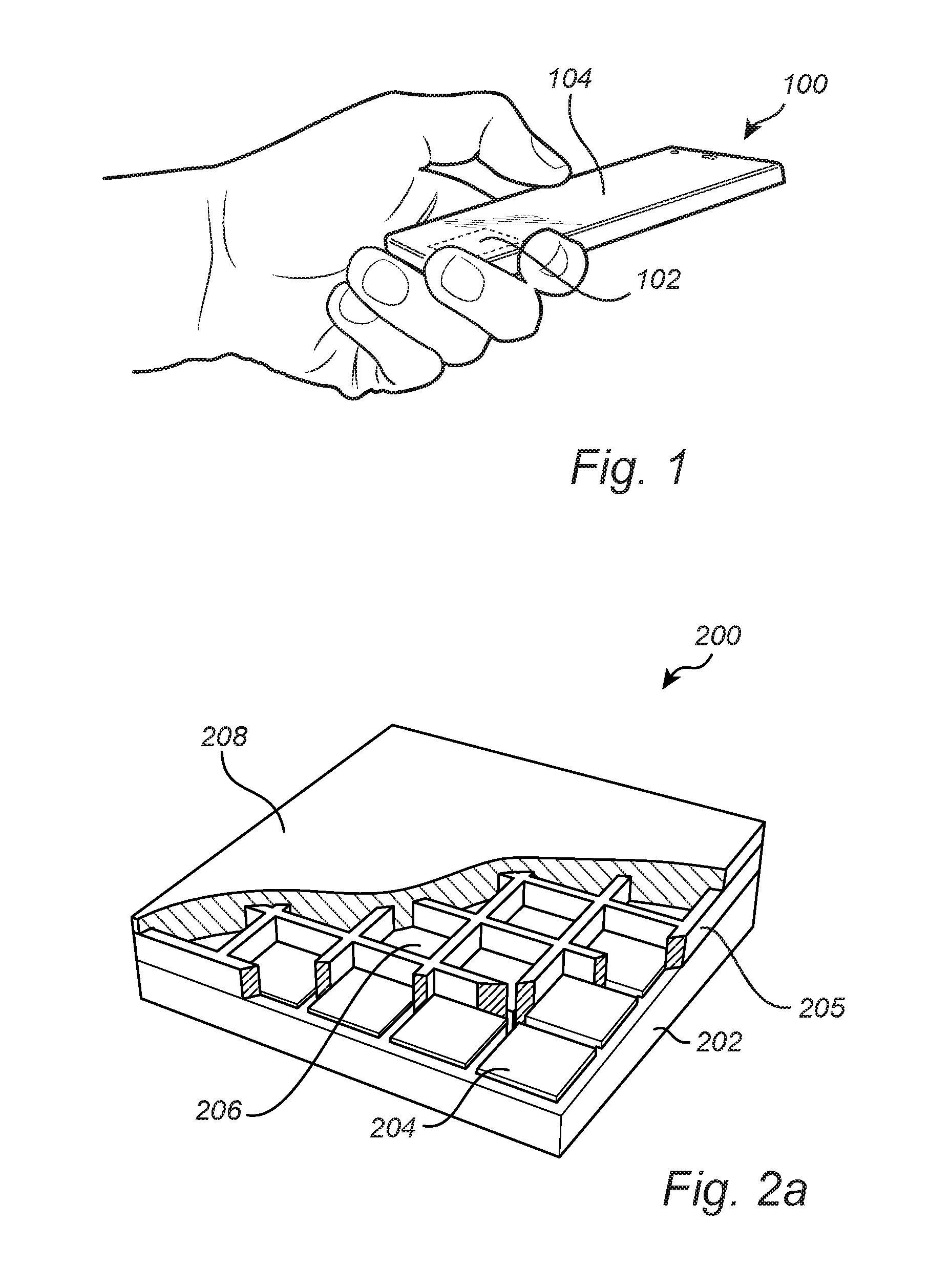
[0051]FIG. 1 is a schematic illustration of a handheld device 100 comprising a fingerprint sensing device 102 comprising a touchscreen display 104. A fingerprint sensing device 102 can be used in for example a mobile phone, a tablet computer, a portable computer or any other electronic device requiring a way to identify and / or authenticate a user.

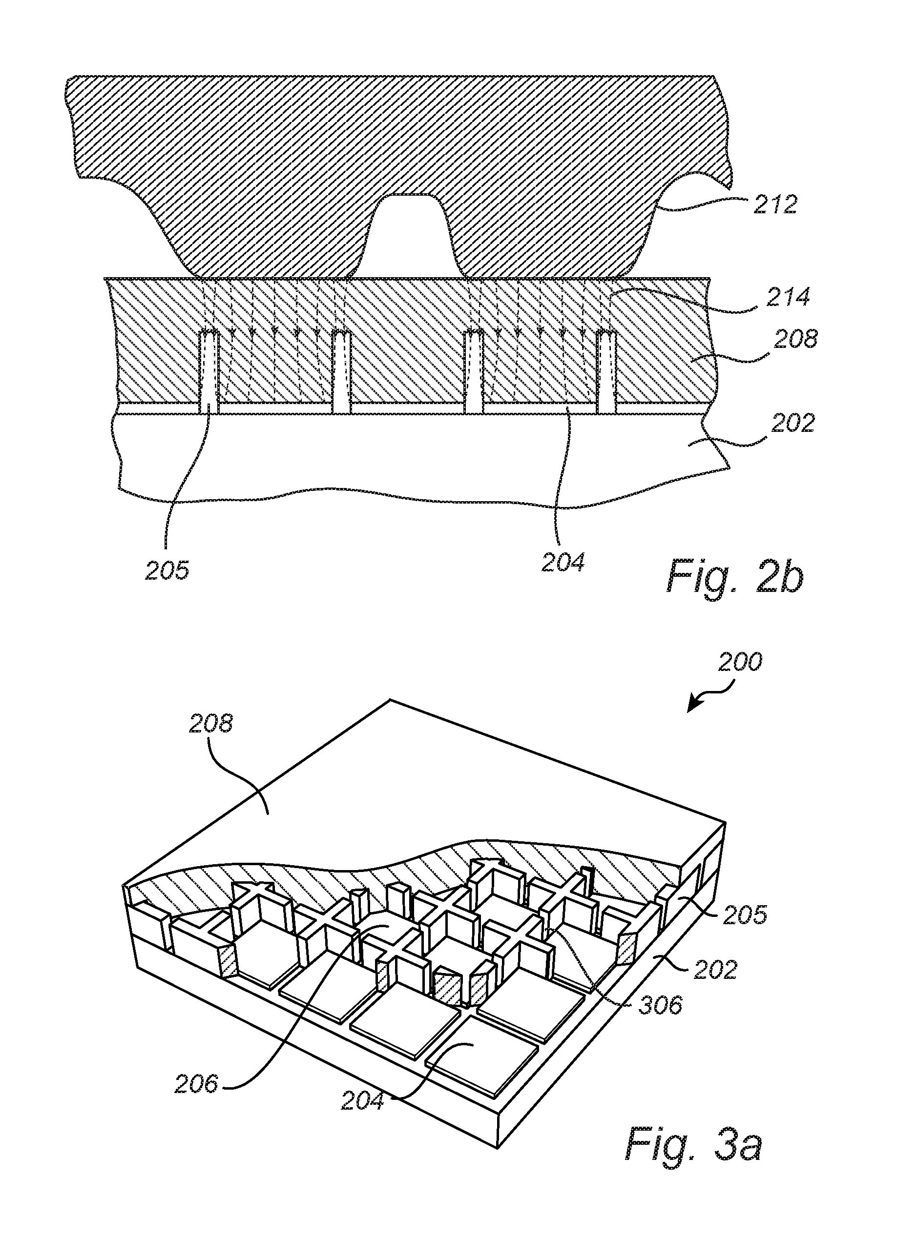
[0052]FIG. 2 is a schematic illustration of a fingerprint sensing device 200 according to an embodiment of the invention. The exterior surface of the sensing device 200 is referred to as the sensing surface, since that is the surface where a finger will be placed for capturing a fingerprint image. The fingerprint sensing device is based on a sensing chip 202 com...


PUM


Abstract

The invention relates to a fingerprint sensing device comprising a sensing chip comprising an array of capacitive sensing elements. The sensing device comprises a coating material arranged in a layer on top of the array of sensing elements, the coating material comprising a plurality of cavities filled with a mold material; wherein locations of the cavities correspond to locations of the sensing elements, such that a cross-section area of a cavity covers at least a portion of an area of a corresponding sensing element; and wherein a dielectric constant of the mold material is higher than a dielectric constant of the coating material. The invention also relates to a method for manufacturing such a device.

Description

CROSS REFERENCE TO RELATED APPLICATIONS[0001]This application claims the benefit of Swedish Patent Application No. 1550749-4 filed Jun. 8, 2015. The disclosure of the above application is incorporated herein by reference in its entirety.FIELD OF THE INVENTION[0002]The present invention relates to a coating structure for a fingerprint sensor. In particular, the present invention related to a heterogeneous coating structure for enhancing the performance in a fingerprint sensor.BACKGROUND OF THE INVENTION[0003]As the development of biometric devices for identity verification, and in particular of fingerprint sensing devices, has lead to devices which are made smaller, cheaper and more energy efficient, the possible applications for such devices are increasing.[0004]In particular fingerprint sensing has been adopted more and more in, for example, consumer electronic devices, due to small form factor, relatively beneficial cost / performance factor and high user acceptance.[0005]Capacitive...

Claims


Application Information

Patent Timeline
IPC IPC(8): B05D1/00B05D1/02G06K9/00G06V40/13
CPCB05D1/005B05D1/02G06K9/00006G06V40/1329G06V40/1306G06F18/00
Inventor LUNDAHL, KARL
Owner FINGERPRINT CARDS ANACATUM IP AB
Why Eureka
Try Eureka