Electrostatic Discharge Power Rail Clamp Circuit
- Summary
- Abstract
- Description
- Claims
- Application Information
AI Technical Summary
Benefits of technology
Problems solved by technology
Method used
Image
Examples
first embodiment
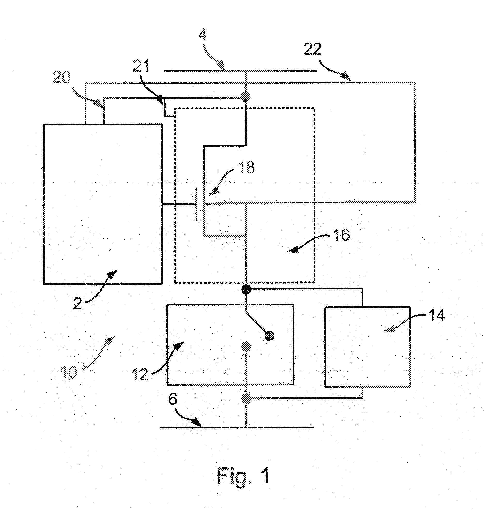
[0044]FIG. 1 shows an electrostatic discharge power rail clamp circuit 10 in accordance with this disclosure. The circuit 10 shown in FIG. 1 includes a first power rail 4 and a second power rail 6. The first power rail 4 may, for instance, provide a supply voltage for a device such as an integrated circuit incorporating the ESD power rail clamp circuit. The second power rail 6 may, for example, be a ground rail. Each of the power rails 4, 6 may be connected to input / output pins of an integrated circuit incorporating the circuit 10.
[0045]The circuit 10 includes an n-channel field effect transistor 18. The field effect transistor 18 is connected between the first power rail 4 and the second power rail 6. During an ESD event, the field effect transistor 18 may be operable to shunt an ESD current from the first power rail 4 to the second power rail 6. The circuit 10 also includes a second ESD device 14, which comprises a silicon controlled rectifier. The second ESD device 14 may be oper...
second embodiment
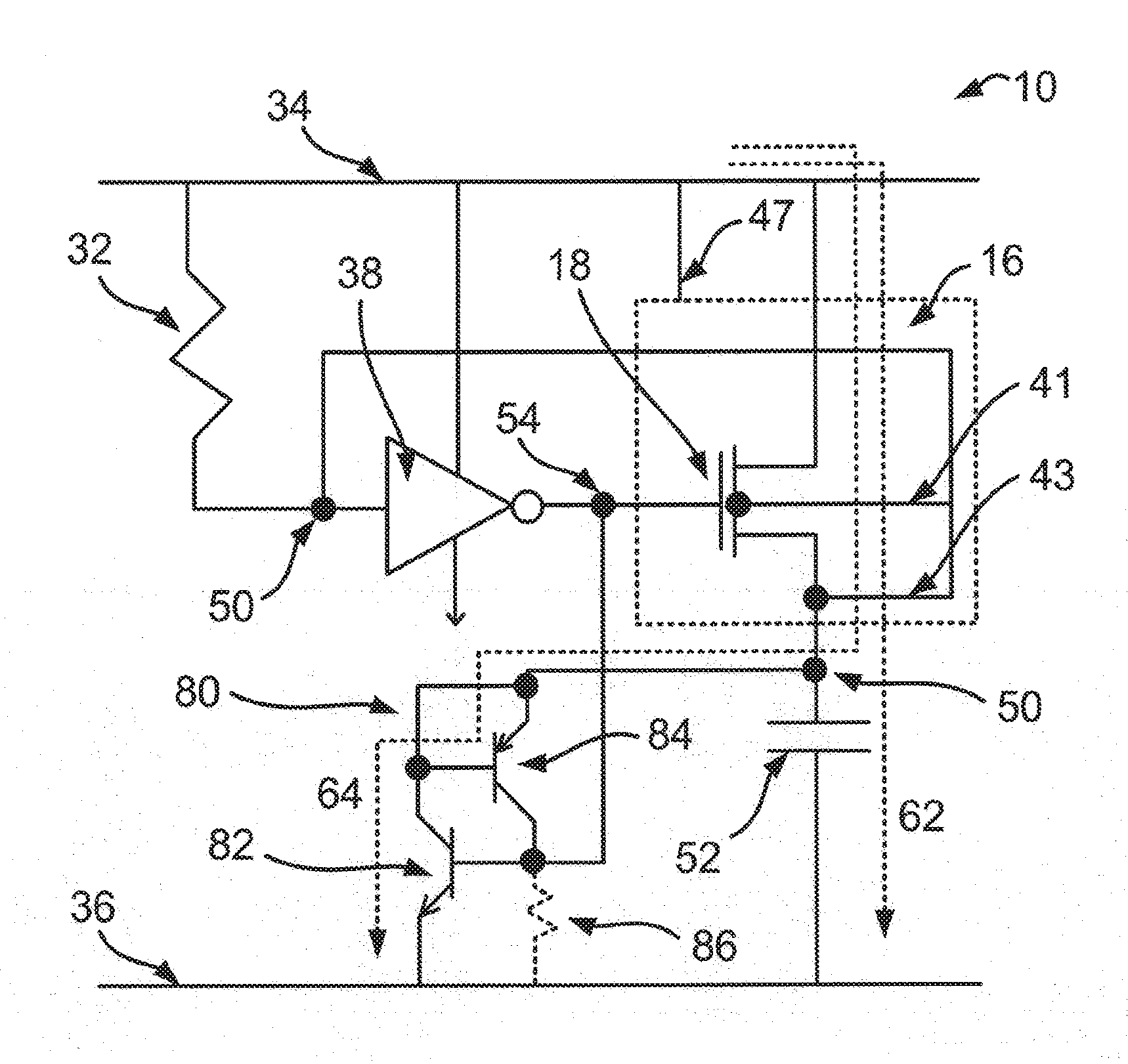
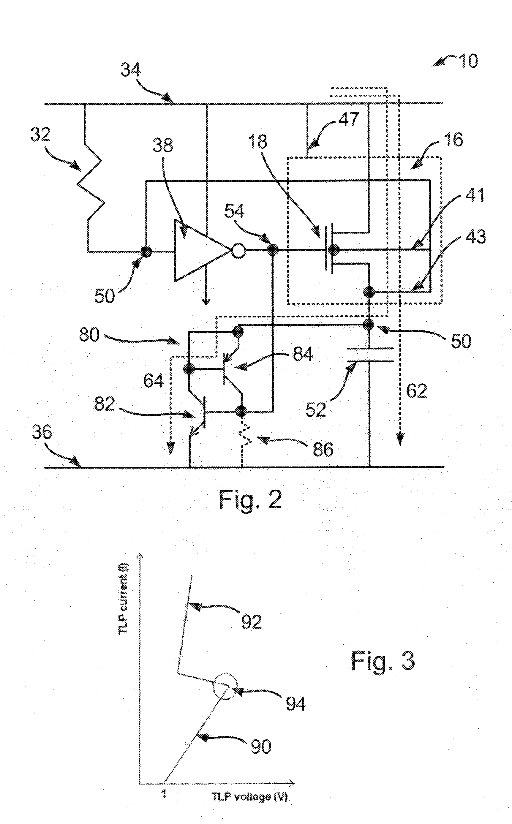
[0052]FIG. 2 shows an electrostatic discharge power rail clamp circuit 10 in accordance with this disclosure. The circuit 10 includes a first power rail 34 and a second power rail 36. The circuit 10 includes a field effect transistor 18. The field effect transistor 18 is an n-channel field effect transistor, which is connected between the first power rail 34 and the second power rail 26 for shunting an ESD current from the first power rail 34 to the second power rail 36 during an ESD event. The drain of the field effect transistor 18 is connected to the first power rail 34. The source of the field effect transistor 18 is connected to a first node 50 of the circuit 10. Note that in FIG. 2 and also in each of the circuit diagrams in the subsequent figures, the first node 50 is shown in two separate locations for reasons of clarity. Although each circuit diagram shows two nodes labelled node 50, these are in fact the same node in the circuit 10.
[0053]As described above, the field effec...
PUM
 Abstract
Description
Claims
Application Information


