Active-matrix touchscreen

a touchscreen and active technology, applied in the field of touchscreen, can solve the problems of large and slow film circuit, and inability to use relatively complex circuits at each pixel location in prior-art lcd or oled display, etc., to achieve the effect of improving performance, reducing size and thickness, and increasing complexity

a touchscreen and active technology, applied in the field of touchscreen, can solve the problems of large and slow film circuit, and inability to use relatively complex circuits at each pixel location in prior-art lcd or oled display, etc., to achieve the effect of improving performance, reducing size and thickness, and increasing complexity

US20170010706A1Active Publication Date: 2017-01-12X DISPLAY CO TECH LTD

Image

  • Active-matrix touchscreen
  • Active-matrix touchscreen
  • Active-matrix touchscreen

Examples


Embodiment Construction

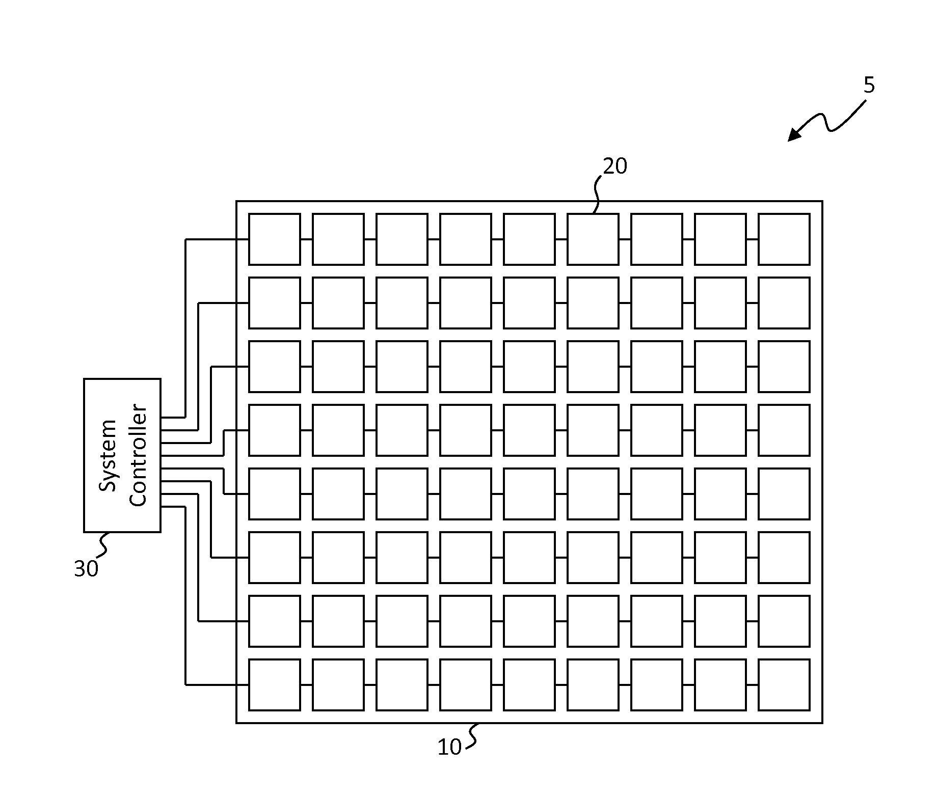
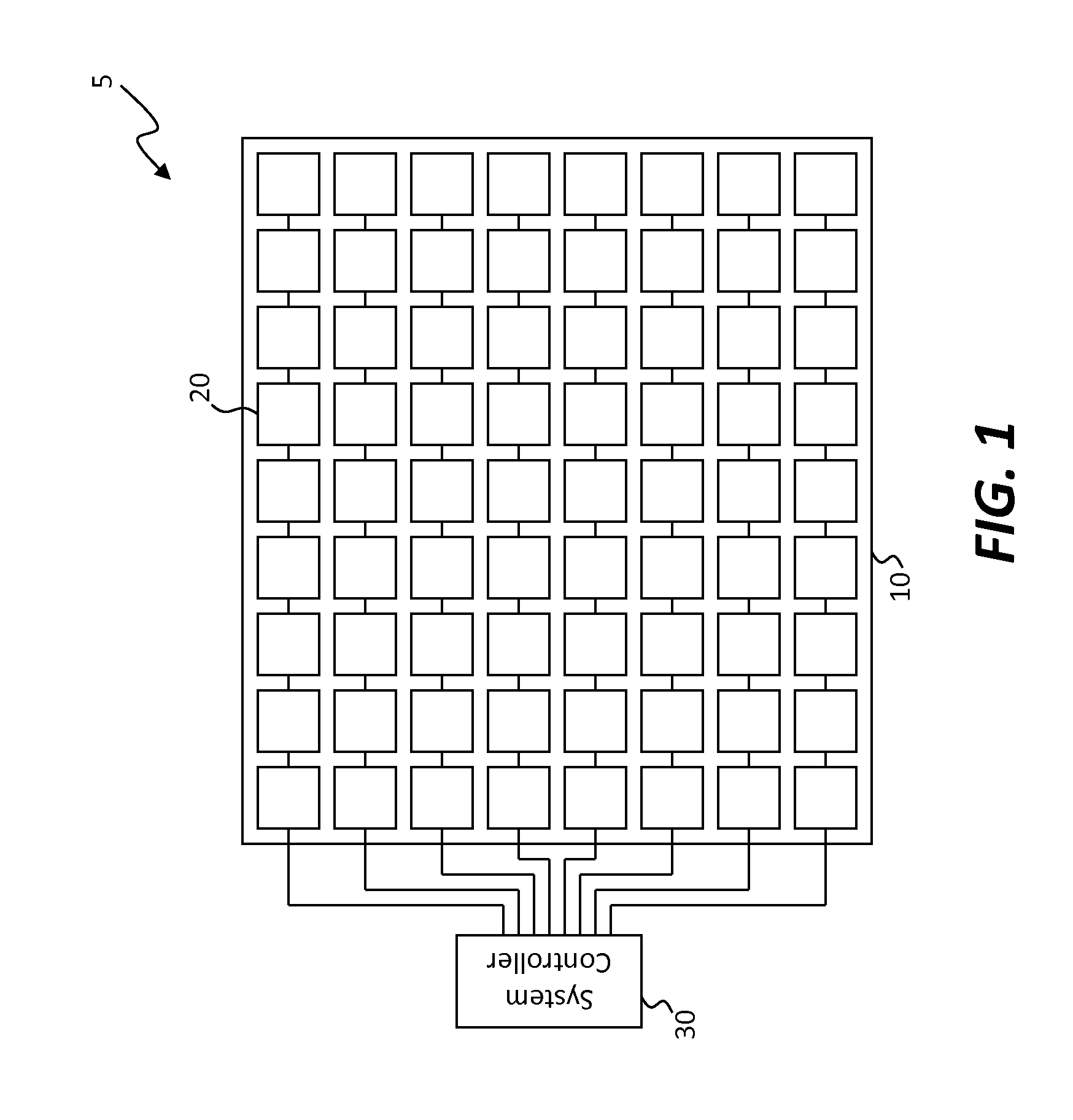
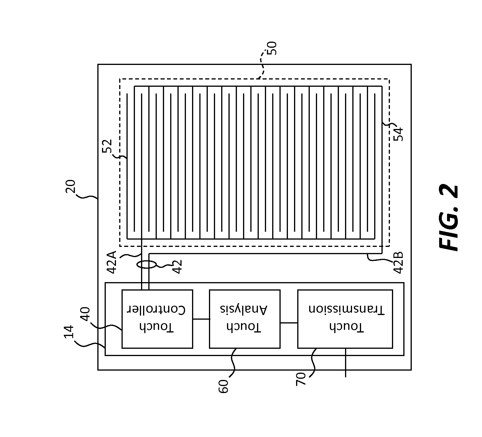
[0152]Referring to the schematic of FIG. 1, in an embodiment of the present invention an active-matrix touchscreen 5 includes a substrate 10 and a system controller 30. The system controller 30 can be located on the substrate 10 or externally to it (as shown) and can, for example, be an integrated circuit. The system controller 30 can be a touch system controller or part of a display system controller, for example also controlling pixels in a display. A plurality of spatially separated independent touch elements 20 are disposed on or over the substrate 10, for example in a two-dimensional arrangement. Referring also to FIG. 2, each touch element 20 includes a touch sensor 50 and a touch controller circuit 40 that provides one or more sensor-control signals 42 to the touch sensor 50 and receives one or more sensor-control signals 42 from the touch sensor 50, for example a sense signal 42B responsive to a drive signal 42A. Each touch sensor 50 operates independently of any other touch...


PUM


Abstract

An active-matrix touchscreen includes a substrate, a system controller, and a plurality of spatially separated independent touch elements disposed on the substrate. Each touch element includes a touch sensor and a touch controller circuit that provides one or more sensor-control signals to the touch sensor and receives a sense signal responsive to the sensor-control signals from the touch sensor. Each touch sensor operates independently of any other touch sensor.

Description

CROSS REFERENCE TO RELATED APPLICATIONS[0001]Reference is made to U.S. patent application Ser. No. 14 / 754,573 filed Jun. 29, 2015, entitled Small Aperture Ratio Display with Electrical Component, U.S. Patent Application Ser. No. 62 / 055,472 filed Sep. 25, 2014, entitled Compound Micro-Assembly Strategies and Devices, and U.S. patent application Ser. No. 14 / 743,981 filed Jun. 18, 2015 and entitled Micro-Assembled Micro LED Displays and Lighting Elements, the contents of each of which is incorporated by reference herein in its entirety.FIELD OF THE INVENTION[0002]The present invention relates to a touchscreen and to a display incorporating such a touchscreen.BACKGROUND OF THE INVENTION[0003]Flat-panel displays are widely used in conjunction with computing devices, in portable devices, and for entertainment devices such as televisions. Such displays typically employ a plurality of pixels distributed over a display substrate to display images, graphics, or text. In a color display, each ...

Claims


Application Information

Patent Timeline
12 Jan 2017
Publication
US20170010706A1
IPC
G06F3/044; G06F3/041
CPC
G06F3/0412; G06F3/044; H01L2224/18; G06F3/04166; G06F2203/04104; G06F3/04164; G06F3/042; H10K50/87
Inventors
COK, RONALD S.