Wear leveling method, memory storage device and memory control circuit unit

Active Publication Date: 2017-01-12
PHISON ELECTRONICS
View PDF5 Cites 8 Cited by
  • Summary
  • Abstract
  • Description
  • Claims
  • Application Information

AI Technical Summary

Benefits of technology

[0009]The present invention provides a wear leveling method, a memory storage device, and a memory control circuit unit ca

Problems solved by technology

Thus, how to select the physical erasing unit for the wear leveling process to make the physical erasing units used evenly and thus effect

Method used


Image

  • Wear leveling method, memory storage device and memory control circuit unit
  • Wear leveling method, memory storage device and memory control circuit unit
  • Wear leveling method, memory storage device and memory control circuit unit

Examples


Example

First Exemplary Embodiment

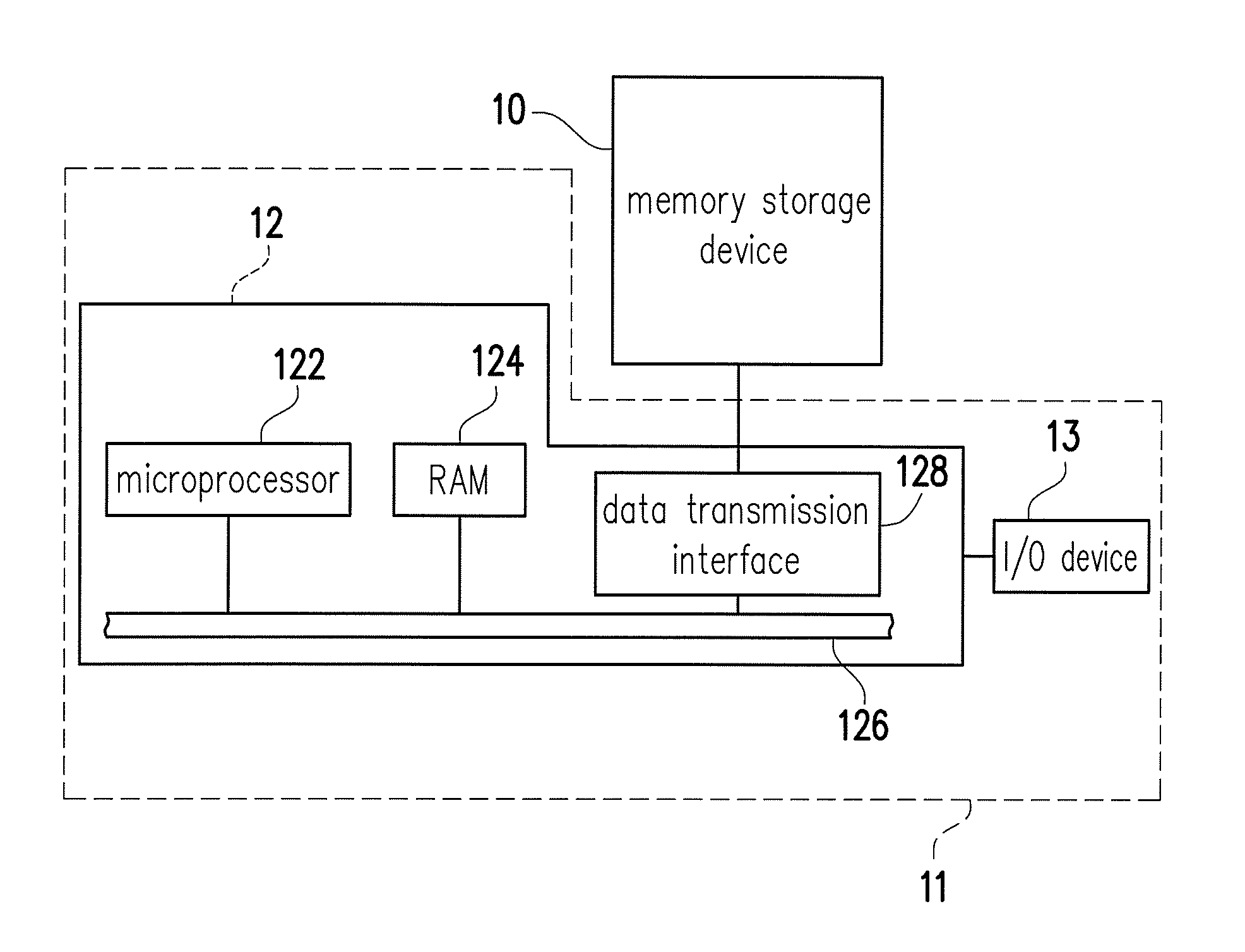
[0033]Generally speaking, a memory storage device (i.e., a memory storage system) includes a rewritable non-volatile memory module and a controller (i.e., a control circuit). The memory storage device is usually used together with a host system, such that the host system can write data into or read data from the memory storage device.

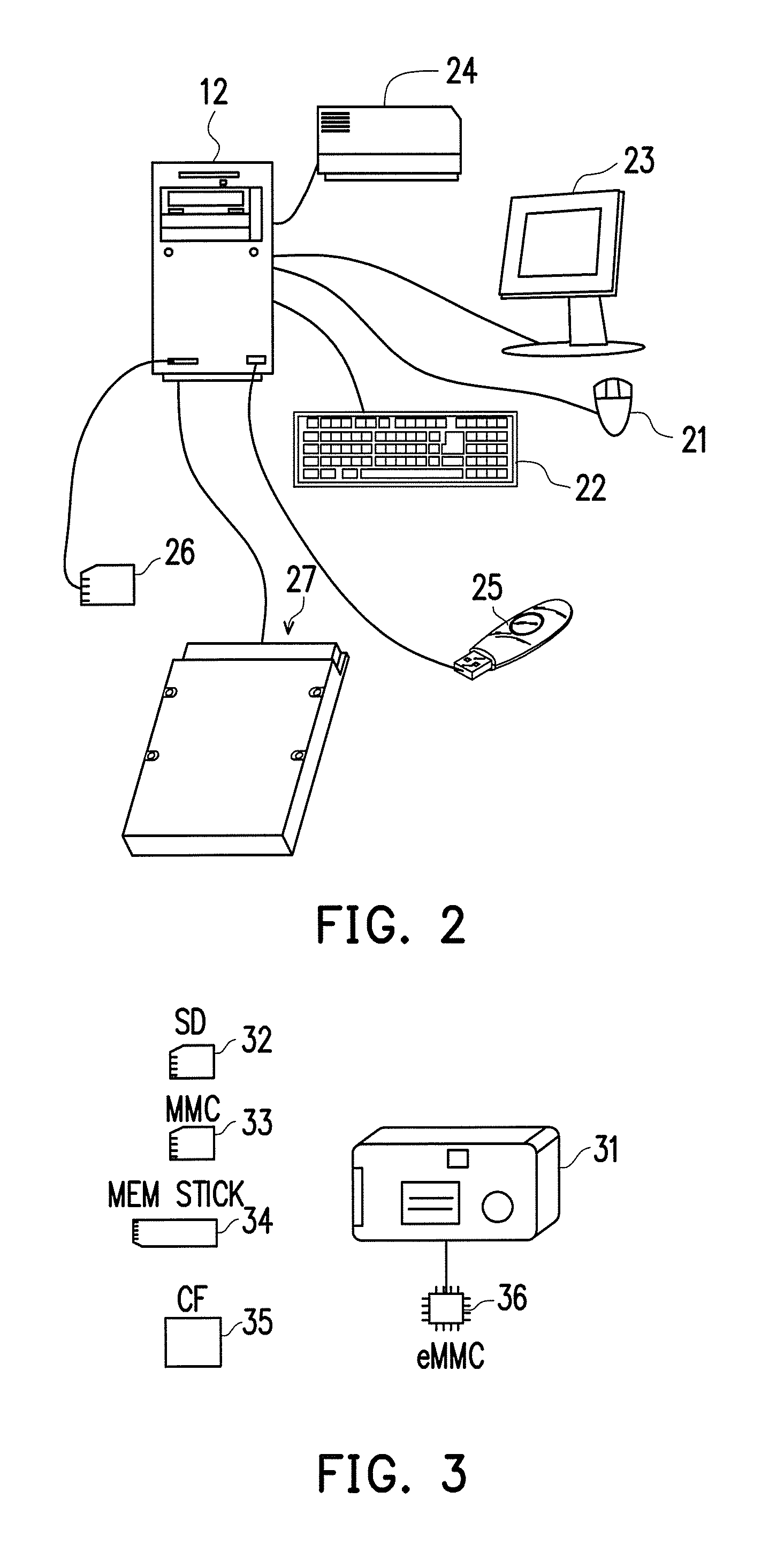
[0034]FIG. 1 is a schematic view illustrating a host system and a memory storage device according to a first exemplary embodiment, and FIG. 2 is a schematic view illustrating a computer, an input / output device, and a memory storage device according to the first exemplary embodiment.

[0035]Referring to FIG. 1, a host system 11 includes a computer 12 and an input / output (I / O) device 1106. The computer 12 includes a microprocessor 122, a random access memory (RAM) 124, a system bus 126, and a data transmission interface 128. The I / O device 13 includes a mouse 21, a keyboard 22, a display 23 and a printer 24 as shown in FIG. 2. It s...

Example

Second Exemplary Embodiment

[0090]The hardware structure of a memory storage device of the second exemplary embodiment is substantially identical to the hardware structure of the memory device of the first exemplary embodiment, but differs in that the memory storage device of the first exemplary embodiment arranges the timestamps for the physical erasing units of the data area as a queue, while the memory storage device of the second exemplary embodiment arranges the timestamps for the physical erasing units of the data area as a programming sequence table. In the following, the operation of the memory storage device of the second exemplary embodiment is described in detail with reference to the figures and reference numerals of the memory storage device of the first exemplary embodiment.

[0091]FIGS. 12A and 12B are schematic views illustrating allocating timestamps for physical erasing units in a data area according to a second exemplary embodiment.

[0092]Referring to FIG. 12A, the me...

Example

Third Exemplary Embodiment

[0097]The hardware structure of a memory storage device of the third exemplary embodiment is substantially the same as the hardware structure of the memory storage device of the first exemplary embodiment, but differs in that the memory storage device of the third exemplary embodiment uses the redundant bit area of the physical erasing unit to record the timestamp for each of the physical erasing units in the data area. In the following, the operation of the memory storage device of the third exemplary embodiment is described in detail with reference to the figures and reference numerals of the memory storage device of the first exemplary embodiment.

[0098]FIGS. 13A and 13B are schematic views illustrating allocating timestamps for physical erasing units in a data area according to a third exemplary embodiment.

[0099]Referring to FIG. 13A, each of the physical erasing units includes a plurality of physical programming units, and each of the programming units ...


PUM


Abstract

A wear leveling method for a rewritable non-volatile memory module is provided. The method includes: recording a timestamp for each of physical erasing units storing valid data according to a programming sequence of the physical erasing units storing valid data among the physical erasing units, and recording an erase count for each of physical erasing units. The method also includes: selecting a first physical erasing unit from the physical erasing units storing valid data according to the timestamps, selecting a second physical erasing unit from physical erasing units not storing valid data among the physical erasing units according to the erase counts, and writing valid data of the first physical erasing unit into the second physical erasing unit, and marking the first physical erasing unit as a physical erasing unit not storing valid data.

Description

CROSS-REFERENCE TO RELATED APPLICATION[0001]This application claims the priority benefit of Taiwan application serial no. 104122031, filed on Jul. 7, 2015. The entirety of the above-mentioned patent application is hereby incorporated by reference herein and made a part of this specification.BACKGROUND[0002]1. Technology Field[0003]The present invention relates to a wear leveling method, and particularly relates to a wear leveling method for a non-volatile memory module, a memory storage device, and a memory control circuit unit.[0004]2. Description of Related Art[0005]The growth of digital cameras, mobile phones, and MP3 players has been rapid in recent years. Consequently, the consumers' demand for storage media has increased tremendously. Since the rewritable non-volatile memory has the characteristics of data non-volatility, low power consumption, compact size, non-mechanical structure, and fast reading / writing speed, the rewritable non-volatile memory has gained its popularity i...

Claims


Application Information

Patent Timeline
IPC IPC(8): G06F12/02G11C16/16
CPCG06F12/0246G06F2212/7211G06F2212/7201G11C16/16G06F2212/1036G06F2212/7205G06F2212/7207G11C16/00G11C16/349G11C16/3495
Inventor TAN, KOK-YONG
Owner PHISON ELECTRONICS
Why Eureka
Try Eureka