

Image device and imaging apparatus
- Summary
- Abstract
- Description
- Claims
- Application Information
AI Technical Summary
Benefits of technology
Problems solved by technology
Method used
Image

Examples
first embodiment
1. First Embodiment
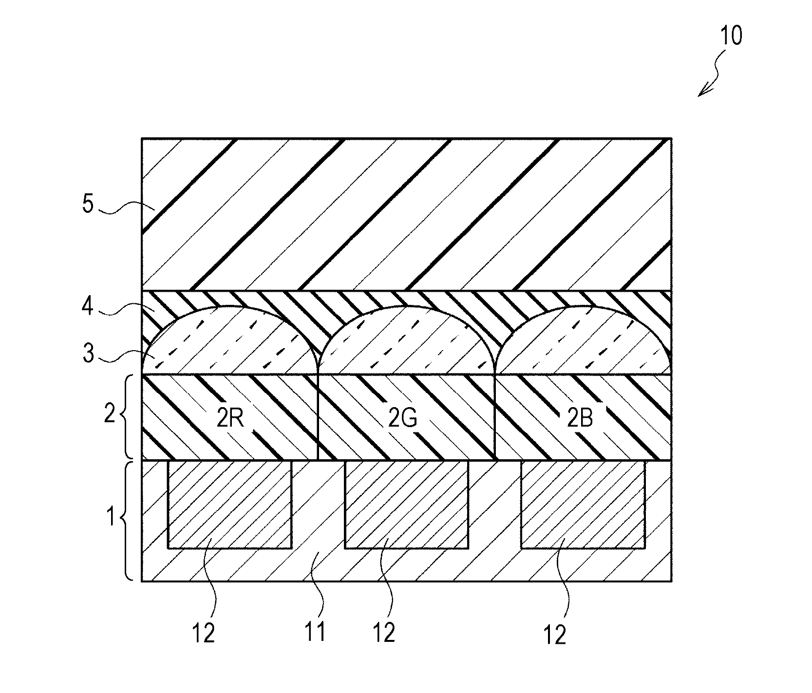
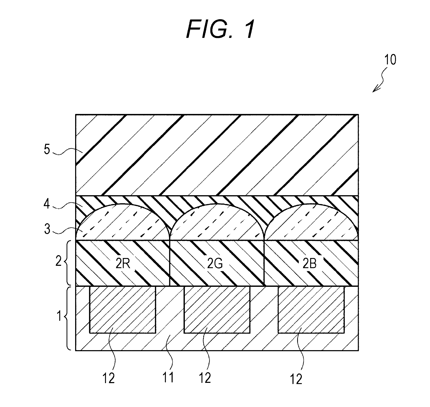
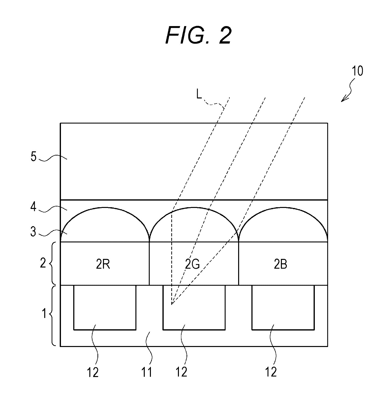
[0033]First, an imaging device according to the first embodiment of the present disclosure will be described. FIG. 1 is a cross-sectional view schematically showing a structure example of an imaging device of the present embodiment. An imaging device 10 of the present embodiment is mounted on an imaging apparatus such as a video camera or a digital still camera, and includes an on-chip lens 3, a planarizing layer 4, and an infrared light absorption layer 5 as shown in FIG. 1. Specifically, in the imaging device 10 of the present embodiment, a color filter layer 2, an on-chip lens 3, planarizing layer 4, and an infrared light absorption layer 5 are formed in this order on a photoelectric conversion layer 1.
[0034]1>
[0035]The photoelectric conversion layer 1 detects the incident light as an electrical signal. For example, a plurality of photoelectric conversion elements 12 is formed on a substrate 11 of silicon or the like. The structure of the photoelectric conversi...
second embodiment
2. Second Embodiment
[0073]Subsequently, an imaging device according to the second embodiment of the present disclosure will be described. FIG. 3 is a cross-sectional view schematically showing a structure example of an imaging device of the present embodiment. Note that, in FIG. 3, structural elements that are the same as the structural element of the imaging device of the first embodiment shown in FIG. 1 are denoted with the same reference numerals, and repeated explanation of these structural elements is omitted.
[0074]
[0075]As shown in FIG. 3, an imaging device 20 of the present embodiment is the same as the imaging device 10 of the first embodiment described above except that the protective layer 6 is formed on the top surface, the side surface or both the surfaces of the infrared light absorption layer 5. Note that although FIG. 3 shows an example in which the protective layer 6 is formed on the infrared light absorption layer 5, the protective layer 6 may be formed only on the ...
third embodiment
3. Third Embodiment
[0079]Subsequently, an imaging device according to the third embodiment of the present disclosure will be described.
[0080]FIG. 4 is a cross-sectional view schematically showing a structure example of an imaging device of the present embodiment. Note that, in FIG. 4, structural elements that are the same as the structural elements of the imaging devices of the first and second embodiments shown in FIGS. 1 and 3 are denoted with the same reference numerals, and repeated explanation of these structural elements is omitted.
[0081]
[0082]As shown in FIG. 4, an imaging device 30 of the present embodiment is the same as the imaging device 20 of the second embodiment described above except that a light antireflection layer 7 is provided on the uppermost layer. Note that although FIG. 4 shows an example of an imaging device including the protective layer 6, the light antireflection layer 7 can also be provided in an imaging device without the protective layer. In that case, ...
PUM
| Property | Measurement | Unit |
|---|---|---|
| Thickness | aaaaa | aaaaa |
| Thickness | aaaaa | aaaaa |
| Wavelength | aaaaa | aaaaa |
Abstract
Description
Claims
Application Information