Method of fabricating semiconductor device

a technology of semiconductor devices and manufacturing methods, applied in semiconductor devices, semiconductor/solid-state device details, electrical equipment, etc., can solve the problems of physical limitation, high cost of design, process development, photomasks, etc., and many traditional process and fabrication methods cannot meet the fabrication requirement anymor

Active Publication Date: 2017-01-26
UNITED MICROELECTRONICS CORP
View PDF7 Cites 2 Cited by
  • Summary
  • Abstract
  • Description
  • Claims
  • Application Information

AI Technical Summary

Benefits of technology

[0009]According to the above, the semiconductor device and the forming method thereof in the present invention mainly replaces a portion of the hard mask layer with the blocking pattern, and then forms the sacrificial patterns and the spacers on the hard mask layer, for blocking a portion of the patterns of the spacers. In this way, the semiconductor device formed accordingly may obtain specific layout. Since the blocki

Problems solved by technology

In recent years, as the continuous decrease of the sizes of semiconductor devices and the increase of the stacking and integration density of semiconductor devices, the photolithography process approaches physical limitation such that the costs of design, process development, and photomask rise dramatically.
Therefore, many traditional process and fabrication method cannot meet the fabrication requiremen

Method used


Image

  • Method of fabricating semiconductor device
  • Method of fabricating semiconductor device
  • Method of fabricating semiconductor device

Examples


Embodiment Construction

[0014]To provide a better understanding of the present invention, preferred embodiments will be described in detail. The preferred embodiments of the present invention are illustrated in the accompanying drawings with numbered elements.

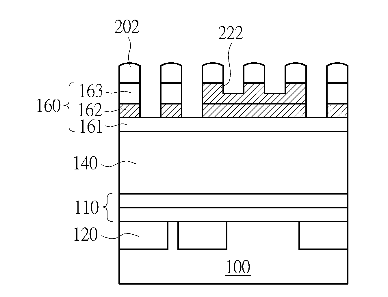
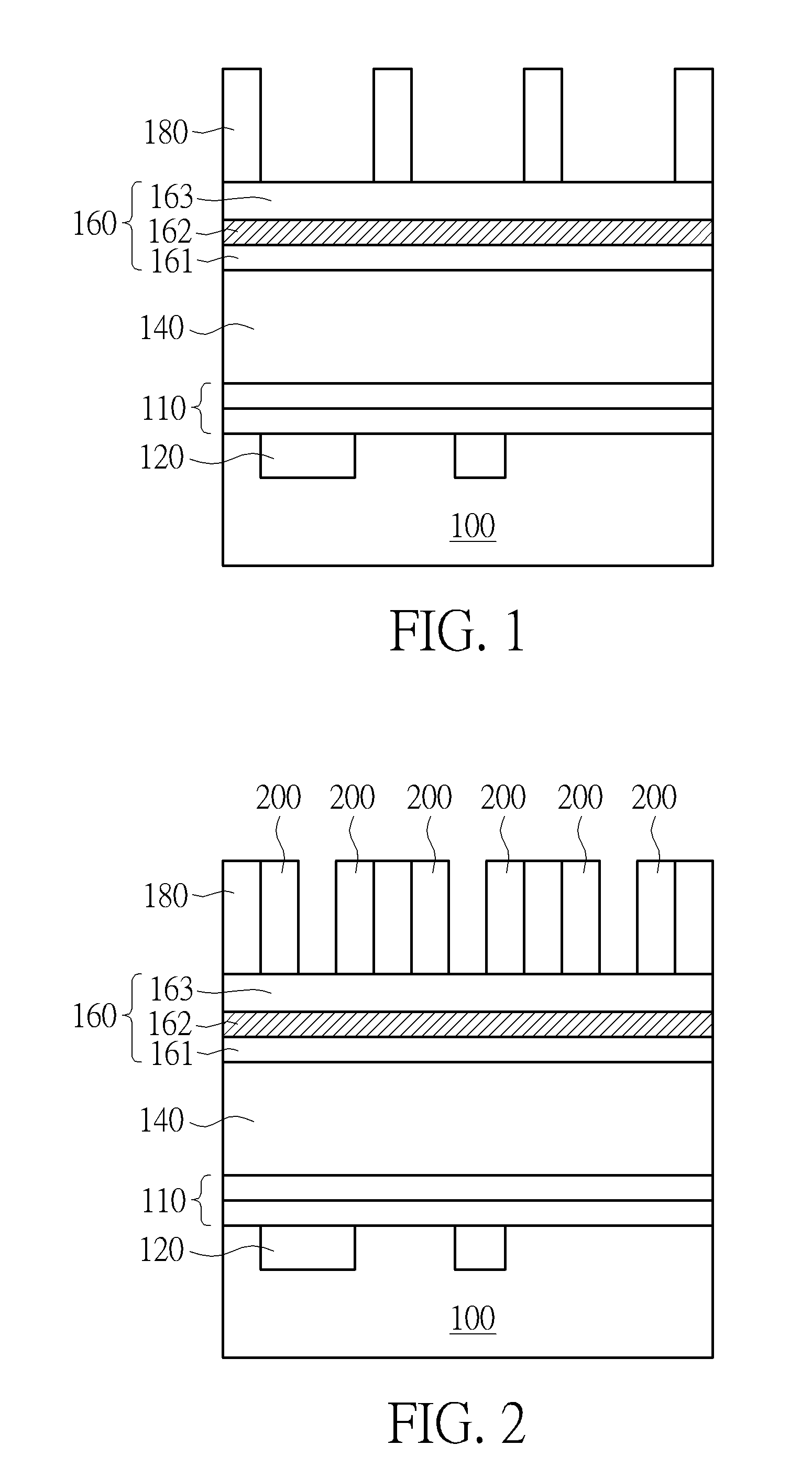
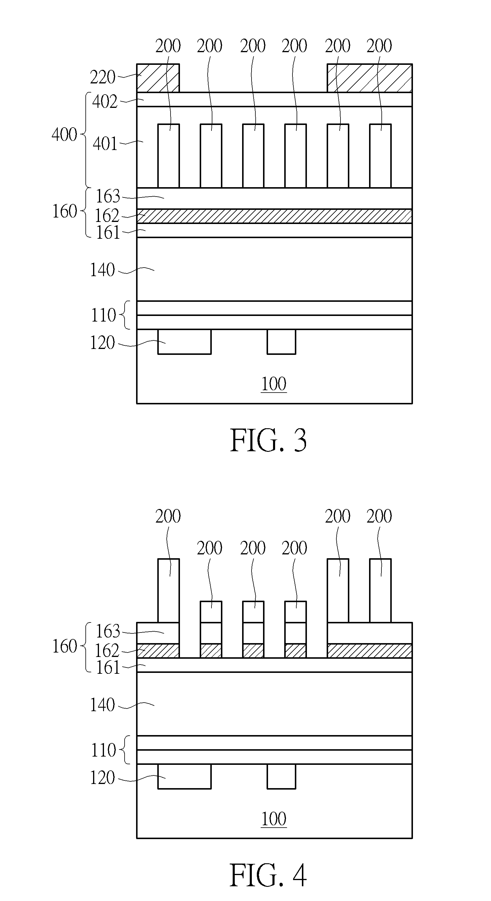
[0015]Please refer to FIG. 1 to FIG. 4, which are schematic diagrams illustrating a method of forming a semiconductor device according to the first embodiment of the present invention. First of all, a substrate 100 is provided. The substrate 100 may include a dielectric material, such as a dielectric layer, as shown in FIG. 1. In one embodiment, the dielectric layer may include a multilayer structure, for example a composite structure consisted of low dielectric constant (low-k) materials (having a dielectric constant less than 3.9), such as silicon oxide, silicon oxynitride and silicon carbonitride, but is not limited thereto. In another embodiment, the substrate 100 may include a semiconductor material, like, a silicon substrate, a silicon-containin...


PUM


Abstract

A semiconductor device and a method of fabricating the same, the semiconductor device includes a hard mask layer and a plurality of spacers. The hard mask layer is disposed on a target layer and has a first material and a second material. The spacers are disposed on the hard mask layer, wherein a first portion of the spacers is disposed on the first material, and a second portion of the spacers is disposed on the second material.

Description

BACKGROUND OF THE INVENTION[0001]1. Field of the Invention[0002]The invention relates to a semiconductor device and a method of forming the same, and more particularly, to a semiconductor device being formed through a sidewall image transference process and a method of forming the same.[0003]2. Description of the Prior Art[0004]In recent years, as the continuous decrease of the sizes of semiconductor devices and the increase of the stacking and integration density of semiconductor devices, the photolithography process approaches physical limitation such that the costs of design, process development, and photomask rise dramatically. Therefore, many traditional process and fabrication method cannot meet the fabrication requirement anymore. In current techniques, in order to achieve sub-lithographic features, an immersion photolithography process in corporation with the argon fluoride (ArF) laser tool is performed for further improve the resolution. In addition, the manufacturer also p...

Claims


Application Information

Patent Timeline
IPC IPC(8): H01L29/66H01L23/535H01L29/06H01L21/768
CPCH01L29/66553H01L29/0657H01L23/535H01L21/76897H01L21/31144H01L21/76816H01L21/0337H01L21/3086
Inventor LIAO, DUAN QUANCHEN, YIKUNTEY, CHING HWA
Owner UNITED MICROELECTRONICS CORP
Why Eureka
Try Eureka