Method for manufacturing coa liquid crystal panel and coa liquid crystal panel

Inactive Publication Date: 2017-02-09
TCL CHINA STAR OPTOELECTRONICS TECH CO LTD
View PDF7 Cites 8 Cited by
  • Summary
  • Abstract
  • Description
  • Claims
  • Application Information

AI Technical Summary

Benefits of technology

The present invention provides a method and panel for manufacturing a color filter on array (COA) liquid crystal panel without the need for an additional black matrix, which simplifies the manufacturing process and increases the aperture ratio, prevents light leakage, and reduces power consumption. The panel has a simple structure, high aperture ratio, and reduced power consumption. The invention addresses the issue of light leakage by using a planarization layer and a pixel electrode layer with lateral and longitudinal borders to self-shield leaking light, eliminating the need for a black matrix. The manufacturing process is simplified, the aperture ratio is increased, and the panel includes a gate terminal and an amorphous silicon layer to shield light and prevent light leakage.

Problems solved by technology

However, in a regular structure of an array substrate, at the site above the location of the TFT, liquid crystal may suffer random orientation due to terrain irregularity and lacking of control voltage.
However, the arrangement of the black matrix 910 causes a loss of a large fraction of aperture ratio.

Method used


Image

  • Method for manufacturing coa liquid crystal panel and coa liquid crystal panel
  • Method for manufacturing coa liquid crystal panel and coa liquid crystal panel
  • Method for manufacturing coa liquid crystal panel and coa liquid crystal panel

Examples


Embodiment Construction

[0055]To further expound the technical solution adopted in the present invention and the advantages thereof, a detailed description is given to a preferred embodiment of the present invention and the attached drawings.

[0056]Referring to FIG. 3, the present invention provides a method for manufacturing a color filter on array (COA) liquid crystal panel, which comprises the following steps:

[0057]Step 1: as shown in FIG. 4, providing an array substrate 1 and a glass substrate 2.

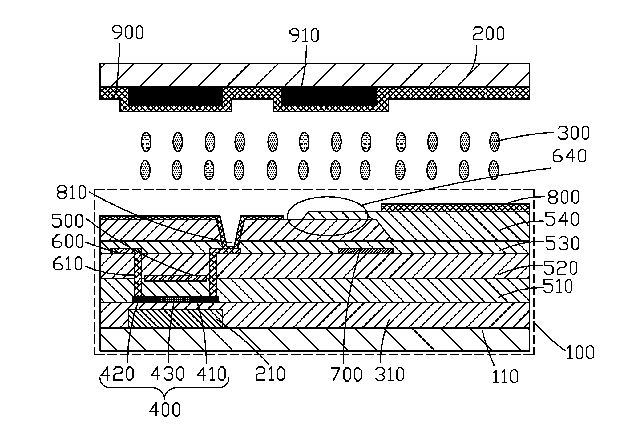
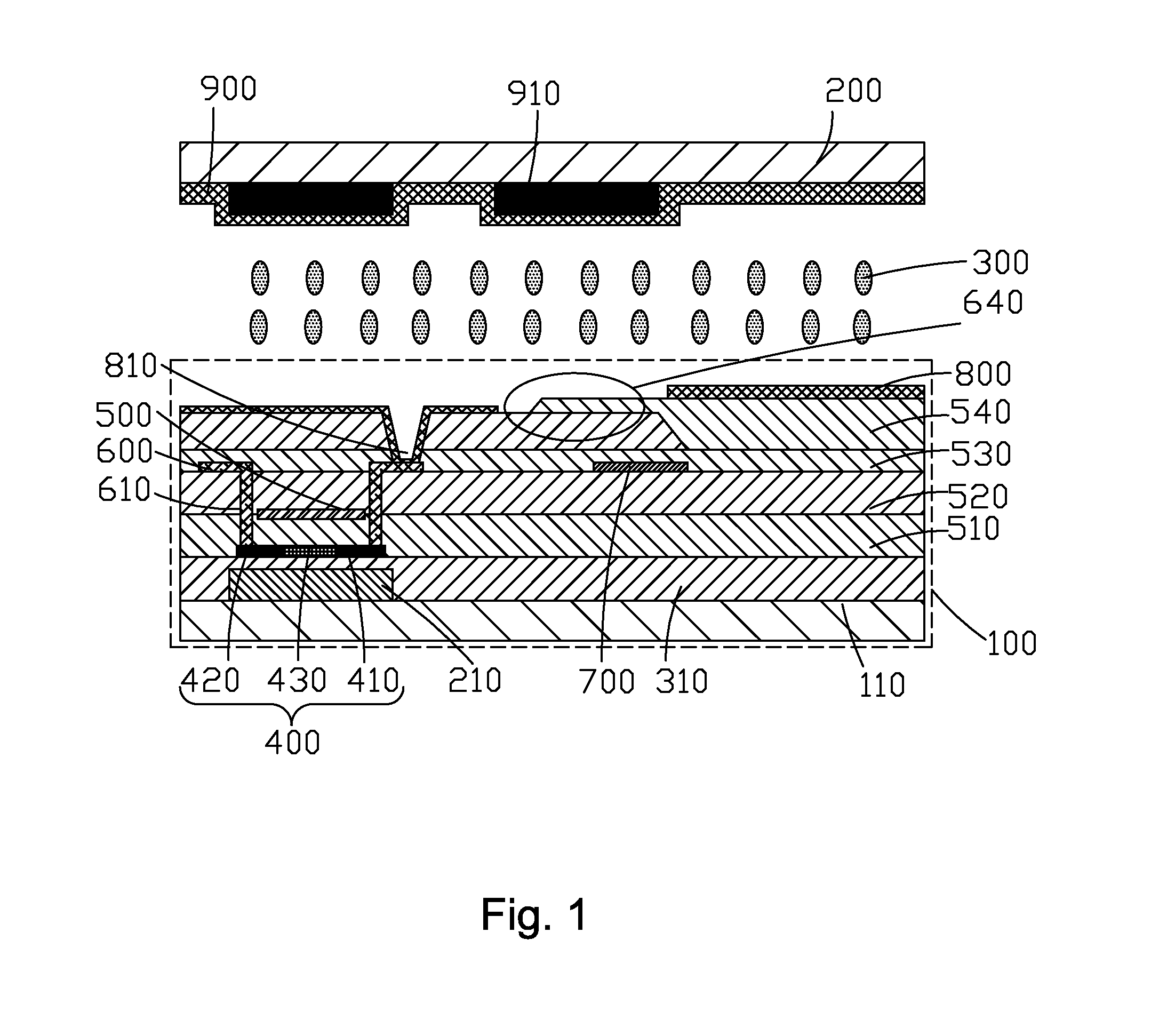
[0058]Specifically, the array substrate 1 comprises red, green, and blue sub pixel zones. Each of the sub pixel zones comprises a base plate 11, an amorphous silicon layer 21 formed on the base plate 11, a buffer layer 31 formed on the amorphous silicon layer 21 and the base plate 11, a poly-silicon layer 4 formed on the buffer layer 31 and corresponding to the amorphous silicon layer 21, a gate insulation layer 51 formed on the poly-silicon layer 4 and the buffer layer 31, a gate terminal 5 formed on the gate i...


PUM


Abstract

The present invention provides a method for manufacturing a COA liquid crystal panel and a COA liquid crystal panel. The method includes forming a planarization layer on a color resist layer to eliminate height difference resulting from stacking or overlapping of adjacent color resist blocks and also includes forming a pixel electrode layer on the planarization layer to set a pixel electrode block thereof located above sub pixel zones in such a way that a lateral border thereof is located above a scan line and a longitudinal border thereof is located above a signal line, whereby the array substrate achieves self-shielding of leaking light in the lateral direction by means of the scan line and also achieve self-shielding of leaking light in the longitudinal direction by means of the signal line and thus no black matrix is necessary is shielding leaking light. As such, the manufacturing process is simplified, the aperture ratio is heightened, and a gate terminal and an amorphous silicon layer are respectively formed on upper and lower sides of the poly-silicon layer to shield light, preventing light leakage from occurring in the site of a channel to affect the liquid crystal layer and also to prevent light leakage caused by misalignment between an array substrate and a glass substrate or panel flexing of a curved display device.

Description

BACKGROUND OF THE INVENTION[0001]1. Field of the Invention[0002]The present invention relates to the field of display technology, and in particular to a method for manufacturing a color filter on array (COA) liquid crystal panel and a COA liquid crystal panel.[0003]2. The Related Arts[0004]Liquid crystal displays (LCDs) have a variety of advantages, such as thin device body, low power consumption, and being free of radiation, and are thus of wide applications, such as liquid crystal televisions, mobile phones, personal digital assistants (PDAs), digital cameras, computer monitors, and notebook computer screens. A liquid crystal display generally comprises an enclosure, a liquid crystal panel arranged in the enclosure, and a backlight module mounted in the enclosure. The liquid crystal panel has a structure that is composed of a thin-film transistor (TFT) array substrate, a color filter (CF) substrate, and a layer of liquid crystal arranged between the two substrates and the operatio...

Claims


Application Information

Patent Timeline
IPC IPC(8): G02F1/1362H01L27/12H01L29/786G02F1/1333G02F1/1343
CPCG02F1/136286G02F2201/123G02F1/136227G02F1/13439H01L29/78633H01L27/124H01L27/1248G02F2001/136222G02F2001/133302G02F2001/134345G02F2202/103G02F2202/104G02F2001/133357G02F2201/52G02F2202/02G02F2201/121G02F1/133345G02F1/133351G02F1/1368H01L29/04G02F1/136209H01L29/78675H01L27/1259G02F1/133357G02F1/136222G02F1/13685G02F1/1362G02F1/133302G02F1/134345
Inventor XU, HONGYUANSUN, BO
Owner TCL CHINA STAR OPTOELECTRONICS TECH CO LTD
Why Eureka
Try Eureka