

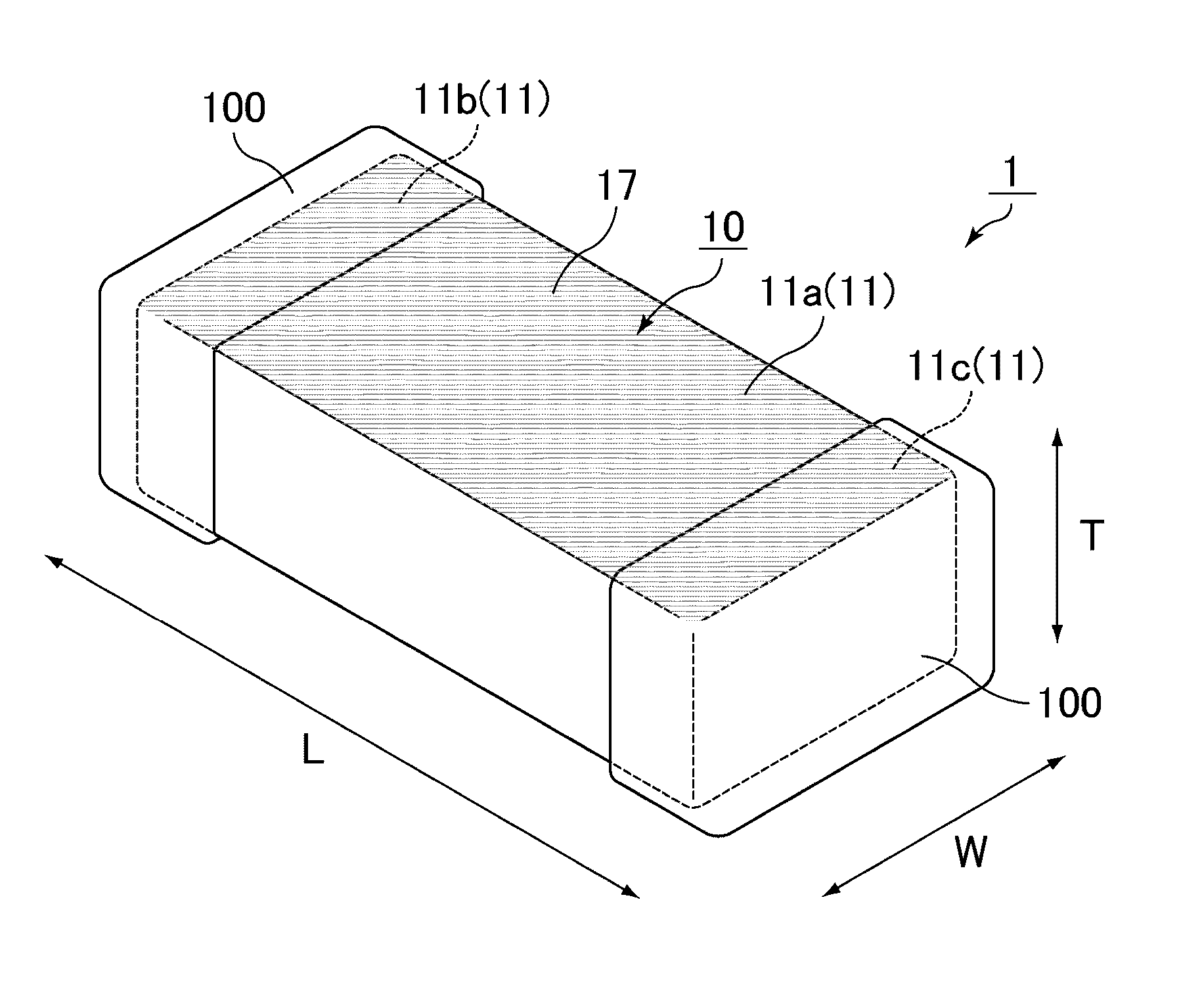
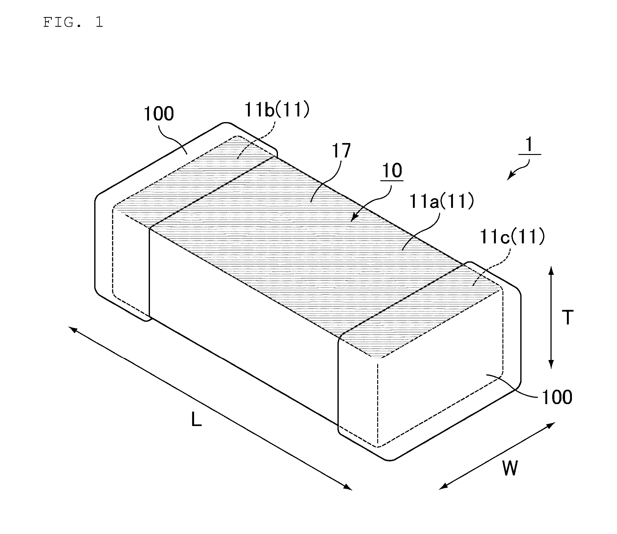
Method of manufacturing ceramic electronic component, and ceramic electronic component
a technology of electronic components and ceramics, applied in the direction of fixed capacitors, stacked capacitors, fixed capacitor details, etc., can solve the problems of reducing the area of connection with through holes, adversely affecting the characteristic adversely affecting the mounting stability of ceramic electronic components, etc., to facilitate through-hole connection and increase fixing strength
- Summary
- Abstract
- Description
- Claims
- Application Information
AI Technical Summary
Benefits of technology
Problems solved by technology
Method used
Image

Examples
example 1
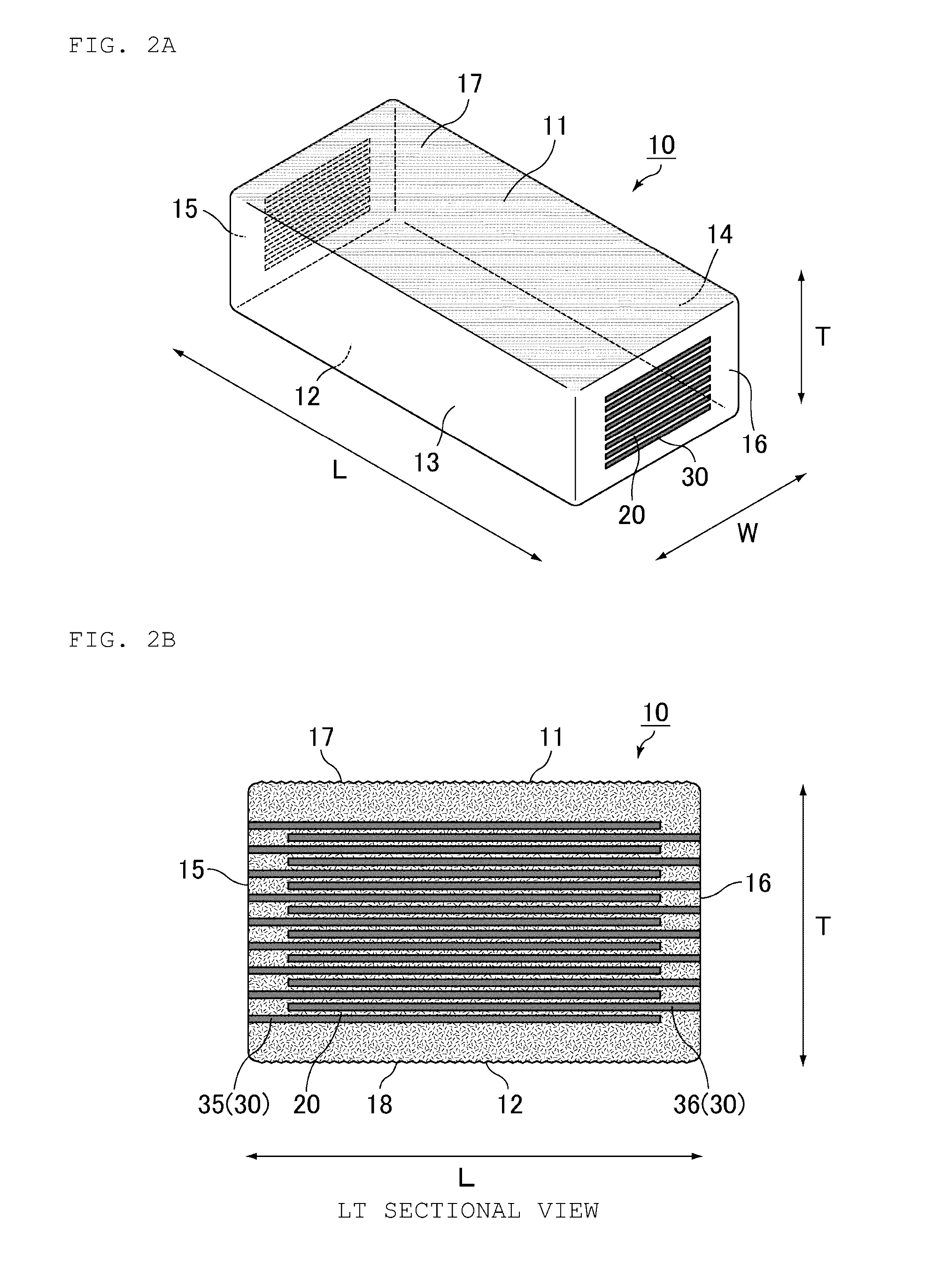
1) Manufacturing of Laminated Block
[0097]A ceramic slurry was manufactured by adding a polyvinyl butyral binder, a plasticizer, and ethanol as an organic solvent to BaTiO3 as a ceramic material, and wet mixing the components with a ball mill. Then, this ceramic slurry was shaped into a sheet by lip coating to acquire a rectangular ceramic sheet. Next, a conductive paste containing Ni was screen printed on the ceramic sheet to form a conductive film serving as an inner conductor layer containing Ni as a primary component. Subsequently, a plurality of ceramic sheets on each of which the conductive film is formed were laminated, so that the conductive films are extended alternately on both sides, to acquire an unprocessed laminated sheet serving as a capacitor main body as illustrated in FIG. 5. Ceramic sheets defining and functioning as the first protection portion and the second protection portion were laminated above and below this unprocessed laminated sheet in an excess amount of ...
PUM
| Property | Measurement | Unit |
|---|---|---|
| thickness | aaaaa | aaaaa |
| thickness | aaaaa | aaaaa |
| thickness | aaaaa | aaaaa |
Abstract
Description
Claims
Application Information