Non-volatile memory and manufacturing method thereof

a non-volatile memory and manufacturing method technology, applied in the field of semiconductor devices, can solve the problems of reduced channel length below, significant influence of electrical performance of memory cells, abnormal punching easily occurring between sources and drains, etc., and achieve the effect of increasing the reliability of semiconductor devices

Active Publication Date: 2017-02-09
IOTMEMORY TECH +2
View PDF8 Cites 16 Cited by
  • Summary
  • Abstract
  • Description
  • Claims
  • Application Information

AI Technical Summary

Benefits of technology

[0008]The invention provides a non-volatile memory and a manufacturing method thereof The non-volatile memory

Problems solved by technology

However, a reduced gate length causes reduction in the channel length below the tunneling oxide layer, and therefore abnormal punch through readily occurs between the source and the drain.
As a result, the electrical performance of the memory cells is

Method used


Image

  • Non-volatile memory and manufacturing method thereof
  • Non-volatile memory and manufacturing method thereof
  • Non-volatile memory and manufacturing method thereof

Examples


Embodiment Construction

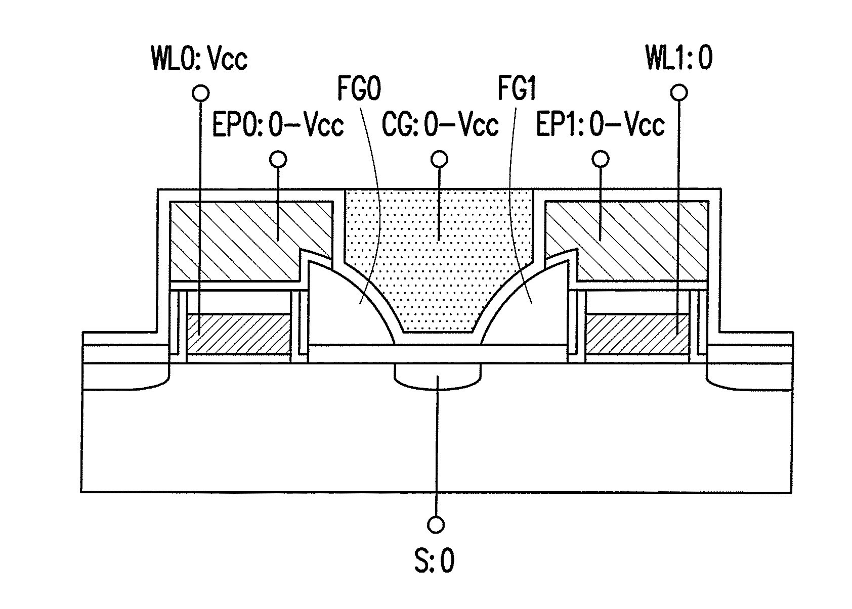
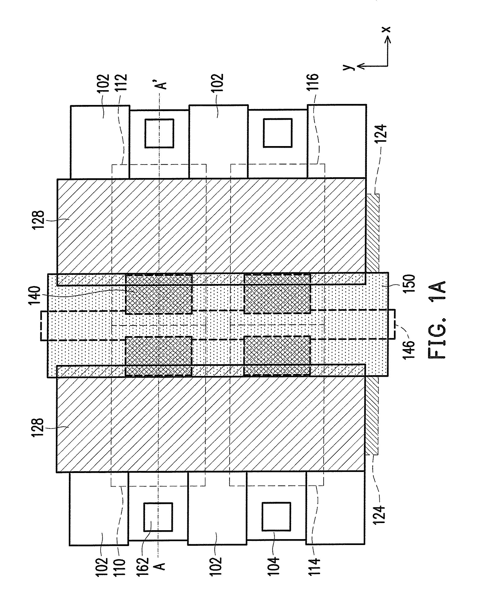
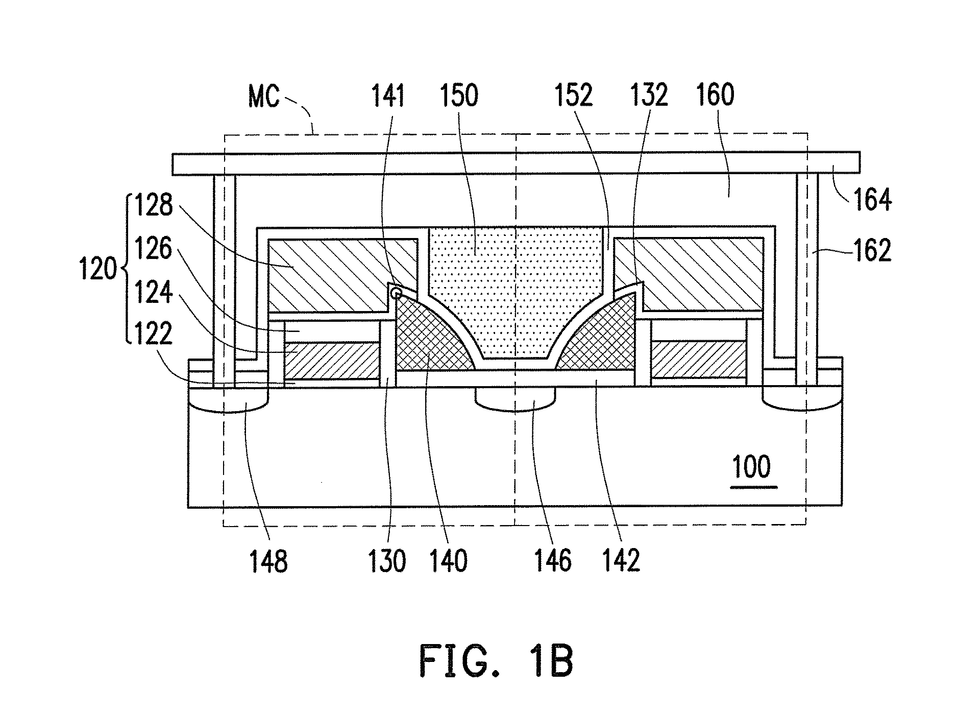
[0036]FIG. 1A is a top view of a non-volatile memory illustrated according to an embodiment of the invention. FIG. 1B is a cross-sectional view of a non-volatile memory illustrated according to an embodiment of the invention. FIG. 1B illustrates a cross-sectional view along line A-A′ in FIG. 1A.

[0037]Referring to FIG. 1A and FIG. 1B, a non-volatile memory includes a plurality of memory cells MC. The memory cells MC are arranged into a row / column array.

[0038]The non-volatile memory is disposed on a substrate 100. A plurality of isolation structures 102 regularly arranged is exemplarily disposed in the substrate 100 to define an active region 104 having a square shape. The isolation structures 102 are, for instance, shallow trench isolation structures.

[0039]Each of the memory cells MC includes a stacked gate structure 120, an assist gate dielectric layer 130, an erase gate dielectric layer 132, a floating gate 140, a tunneling dielectric layer 142, a source region 146, a drain region ...


PUM


Abstract

A non-volatile memory having memory cells is provided. A stacked gate structure has gate dielectric layer, assist gate, insulation layer, and erase gate disposed in order. The floating gate is disposed on a first sidewall of the stacked gate structure, the floating gate has a corner portion at the top portion, and erase gate covers the corner portion. The tunneling dielectric layer is disposed under the floating gate. The erase gate dielectric layer is disposed between the erase gate and the floating gate. The assist gate dielectric layer is disposed between the assist gate and the floating gate. The source region and the drain region are respectively disposed at two sides of the stacked structure and the floating gate. The control gate is disposed on the source region and the floating gate. The inter-gate dielectric layer is disposed between the control gate and the floating gate.

Description

BACKGROUND OF THE INVENTION[0001]Field of the Invention[0002]The invention relates to a semiconductor device and a manufacturing method thereof. More particularly, the invention relates to a non-volatile memory and a manufacturing method thereof.[0003]Description of Related Art[0004]Since a non-volatile memory can, for instance, repeatedly perform operations such as storing, reading, and erasing data, and since stored data is not lost after the non-volatile memory is shut down, the non-volatile memory has been extensively applied in personal computers and electronic equipment.[0005]A traditional structure of non-volatile memory has a stack-gate structure, including a tunneling oxide layer, a floating gate, an inter-gate dielectric layer, and a control gate disposed on a substrate in order. When a programming or erasing operation is performed on such a flash memory device, a suitable voltage is respectively applied to the source region, the drain region, and the control gate, such th...

Claims


Application Information

Patent Timeline
IPC IPC(8): H01L27/115
CPCH01L27/11524H01L28/00H10B41/35H10B43/27
Inventor CHENG, TZUNG-WENCHENG, YU-MING
Owner IOTMEMORY TECH
Why Eureka
Try Eureka