Laser Diode Array Based Photopolymer Exposure System

a photopolymer and laser diode technology, applied in the field of 3d printing, can solve the problems of low power of low-power laser diodes, limiting factors in this process, high-power uv lasers are expensive, etc., and achieve the effects of simplified optical design, reduced cost and simplified optical design

Inactive Publication Date: 2017-02-23
GELBART DANIEL
View PDF4 Cites 8 Cited by
  • Summary
  • Abstract
  • Description
  • Claims
  • Application Information

AI Technical Summary

Benefits of technology

[0003]The invention uses a scanned two dimensional array of single mode laser diodes to generate a large number of beams scanning a large area of liquid photopolymer. The optical design is further simplified by using interleaved scanning generated by tilting a glass plate. Using a wavelength of 405-410 nm allows the use of low cost laser diodes and a simplified optical design.

Problems solved by technology

For full description see : http: / / en.wikipedia.org / wiki / Stereolithography One of the limiting factors in this process is the amount of light, particularly blue or UV light, that can be supplied to cure the photopolymer.
High power UV lasers are expensive, while low cost laser diodes have low power and it is difficult to arrange a large number of them to generate closely spaced tracks.

Method used


Image

  • Laser Diode Array Based Photopolymer Exposure System
  • Laser Diode Array Based Photopolymer Exposure System
  • Laser Diode Array Based Photopolymer Exposure System

Examples


Embodiment Construction

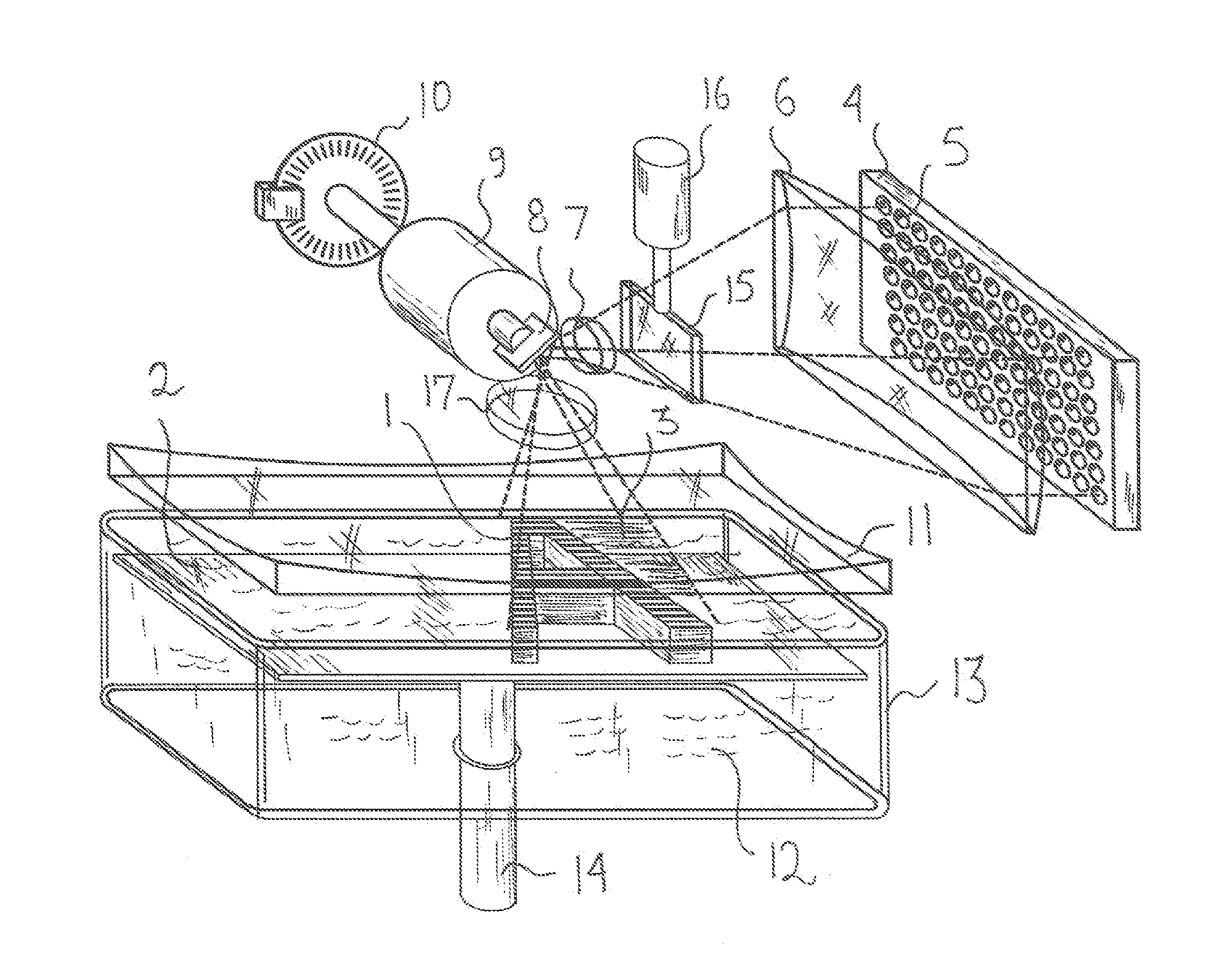
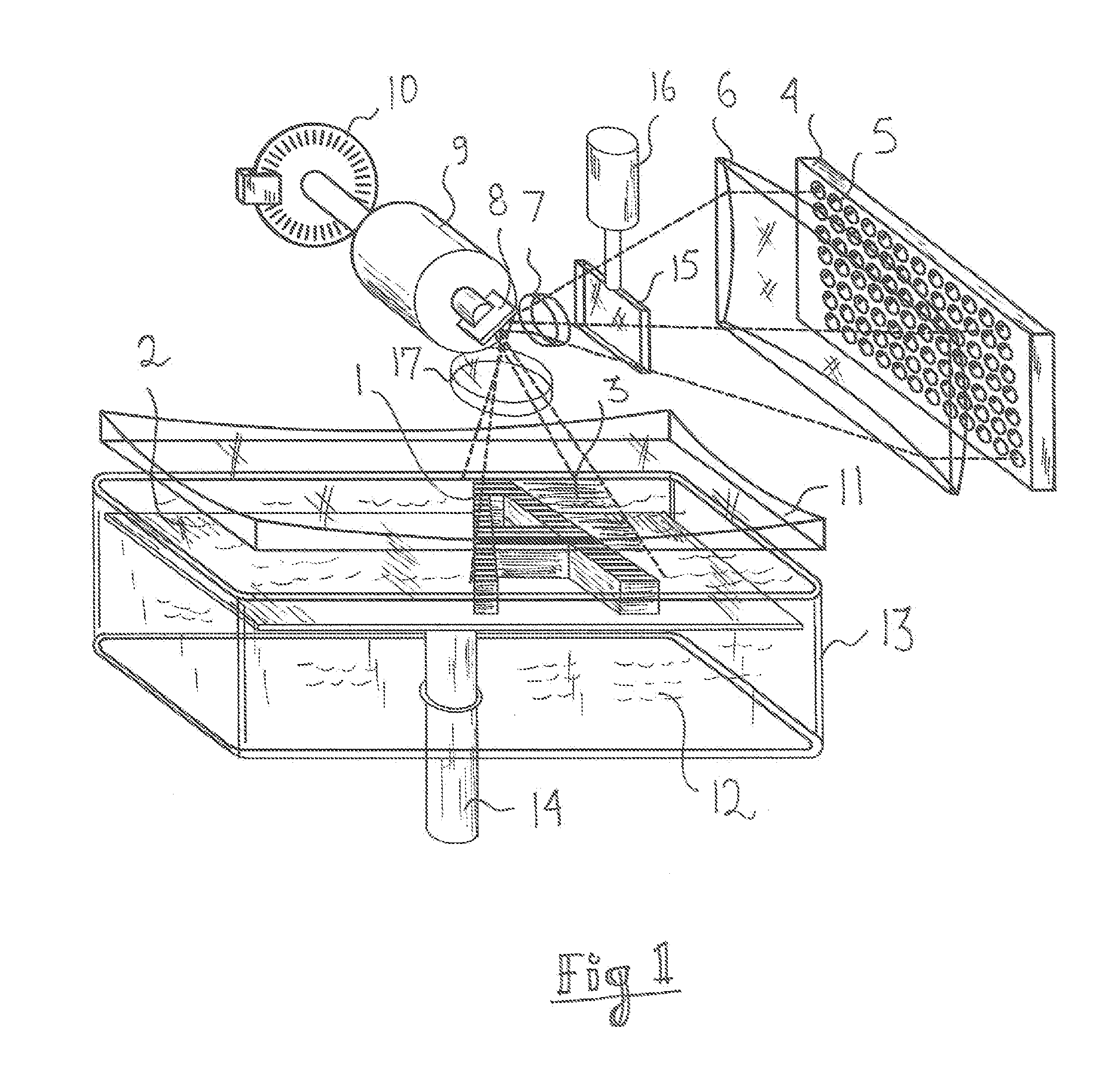
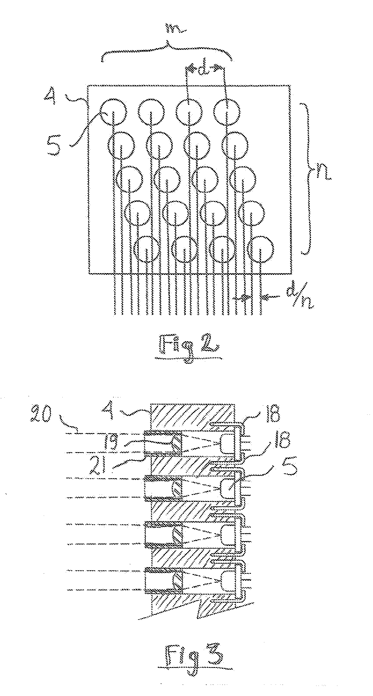
[0014]In order to make an efficient use of the optical field-of-view of the scanning system, a two dimensional array of single mode laser diodes is used as a multi-beam source for image-wise exposing the surface of the liquid photopolymer. The principle of such an array is disclosed in U.S. Pat. No. 4,743,091, hereby incorporated by reference. The principle is also shown in FIG. 2. An array 4 has a 2D array of laser diodes 5. Since each row is shifted relative to the previous one, an array having m columns and n rows will create m×n equally spaced lines when scanned. Furthermore, if the pitch of the laser diodes is d the line spacing will be d / n. This reduces the need for a strong optical image reduction as the actual pitch of the lines in stereolithographe is in typically in the range of 25 um to 250 um. The best utilization of the optics is when m=n, however other ratios can be chosen to maximize throughput. An illustrative example will be described for a system having a resolutio...


PUM

PropertyMeasurementUnit
wavelengthaaaaaaaaaa

Abstract

The invention uses a scanned two dimensional array of single mode laser diodes to generate a large number of beams scanning a large area of liquid photopolymer. The optical design is further simplified by using interleaved scanning generated by tilring a glass plate. Using a wavelength of 405-410nm allows the use of low cost laser diodes and a simplified optical design.

Description

FIELD OF THE INVENTION[0001]The invention is mainly in the field of 3D printing, and specifically for stereolithography.BACKGROUND OF THE INVENTION[0002]Stereolitography, also known as SLA, is a well known method of additive manufacturing or 3D printing. For full description see : http: / / en.wikipedia.org / wiki / Stereolithography One of the limiting factors in this process is the amount of light, particularly blue or UV light, that can be supplied to cure the photopolymer. High power UV lasers are expensive, while low cost laser diodes have low power and it is difficult to arrange a large number of them to generate closely spaced tracks. One object of the invention is to combine a large number of relatively low power diodes to achieve a high power delivered at a high resolution and large number of tracks. It is also desirable to scan a large area of liquid photopolymer without moving the liquid photopolymer, and preferably without moving the laser source. Prior art used deformable mirr...

Claims


Application Information

Patent Timeline
Patent Type & Authority Applications(United States)
IPC IPC(8): B29C67/00H01S5/00H01S5/40
CPCB29C67/0085H01S5/4025B33Y30/00B29C67/0066B29C67/0077H01S5/005B29C64/135B29C64/153B29C64/277B29C64/268
Inventor GELBART, DANIEL
Owner GELBART DANIEL
Why Eureka
Try Eureka