Wafer structure and processing method thereof

a technology of wafer structure and processing method, which is applied in the direction of semiconductor electrostatic transducers, semiconductor/solid-state device testing/measurement, loudspeakers, etc., can solve the problems of failure of die singulation, damage to the die, and difficult penetration of the functional layer of the wafer, so as to improve the yield of the die, reduce manufacturing costs and die costs, and improve the intensity of the wafer structure

Inactive Publication Date: 2017-02-23
ACUTI MICROSYST
View PDF3 Cites 7 Cited by
  • Summary
  • Abstract
  • Description
  • Claims
  • Application Information

AI Technical Summary

Benefits of technology

[0043]In the preferred embodiment, the wafer structure forms the scribing marks in the scribe lane below the functional layer, so that a substantially complete path is generated by the plurality of the scribing marks and the initial cracks, where the initial cracks are formed by the laser scanning. Thus, the adjacent ones of the dies will be singulated by laser cutting conveniently and the die yield will be improved.
[0044]In the preferred embodiment, the first sacrificial layer is used for improving the intensity of the wafer structure in manufacturing process, thus protecting the wafer structure and the manufacturing equipment.
[0045]In the preferred embodiment, the scribing marks with predetermined width and length reduces the frequency of self-testing alignment accuracy in the dicing equipment and thus reducing the manufacturing costs and the die costs.
[0046]In the preferred embodiment, the scribing marks and the acoustic cavity are formed simultaneously in the semiconductor substrate, by selectively etching over a first sacrificial layer having a predetermined thickness. The portion of the first sacrificial layer above the scribing marks remains after etching, for providing strength of the dies after the laser cutting. The thickness of the first sacrificial layer is controlled in a predetermined range to prevent the wafer structure from breaking during processing and transporting, and to prevent the wafer structure from distortion due to a too large thickness of the first sacrificial layer. Thus, a higher die yield is obtained.

Problems solved by technology

The disadvantage of the laser cutting is that the functional layers on the wafer are hard to be penetrated.
However, if the functional layer is formed in the scribe lane, it will be difficult to form the initial cracks continuously in the scribing line due to the blocking by the functional layer, which will lead to a failure on die singulation and even cause damages to the dies.

Method used


Image

  • Wafer structure and processing method thereof
  • Wafer structure and processing method thereof
  • Wafer structure and processing method thereof

Examples


first embodiment

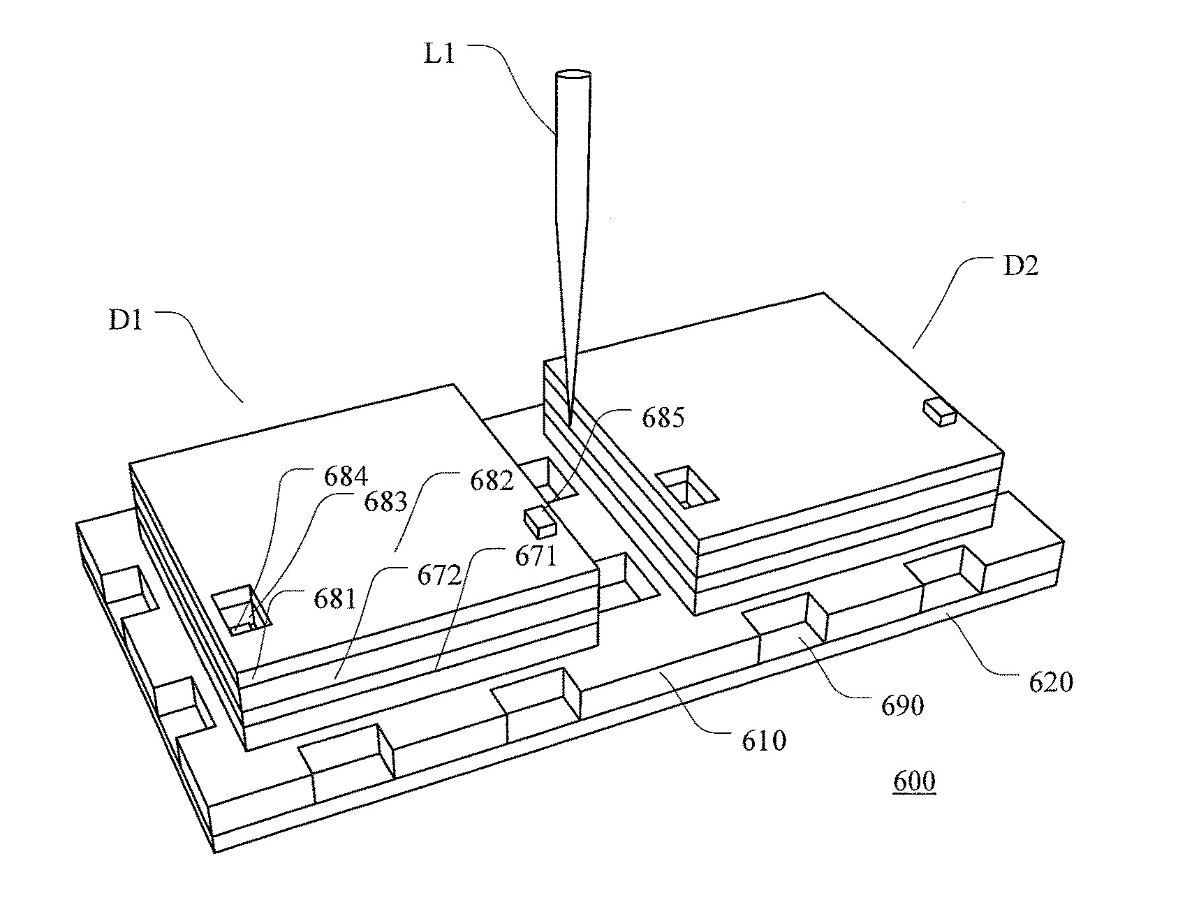
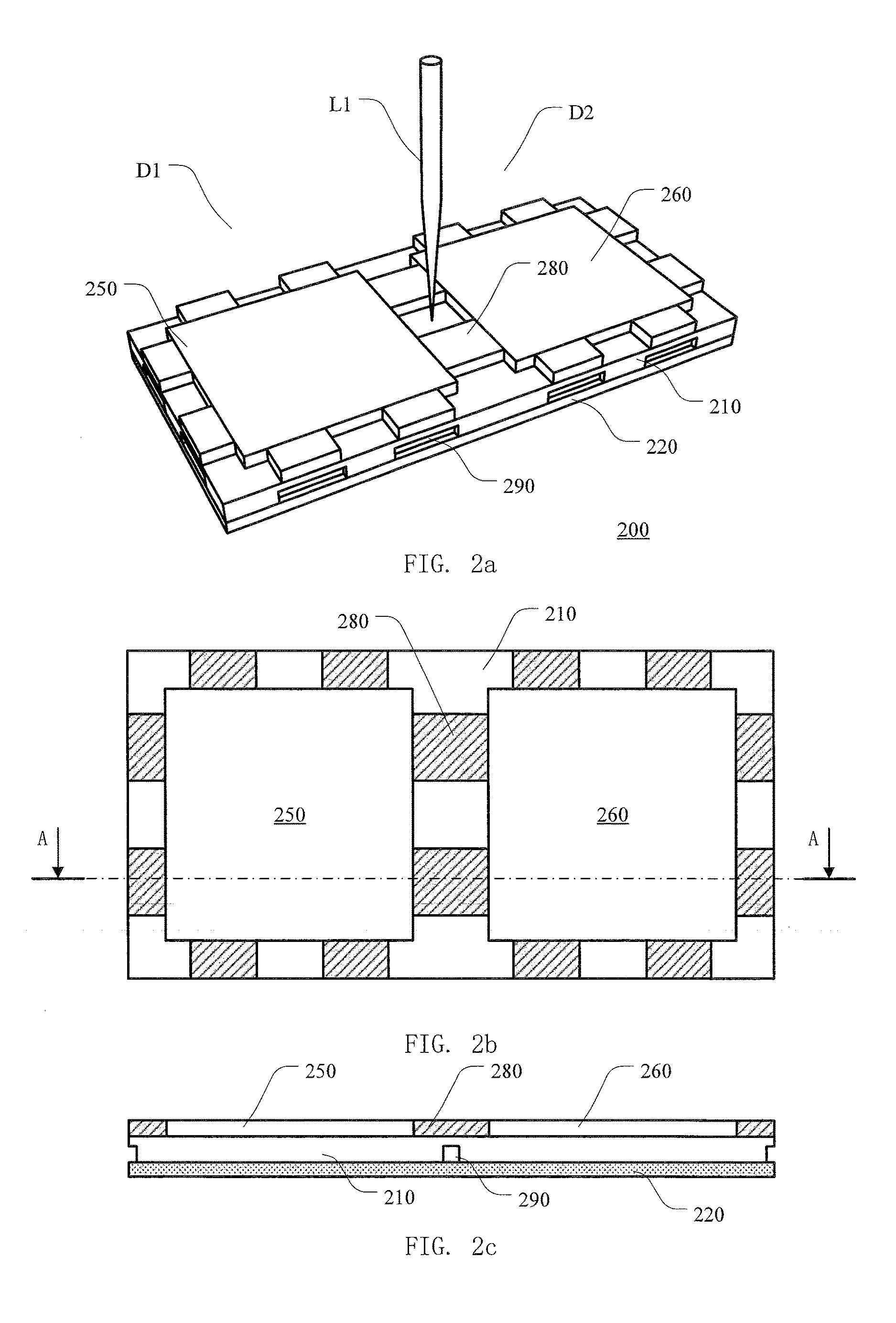
[0068]FIG. 2a to FIG. 2c illustrate schematic diagrams of a wafer structure according to the disclosure in a perspective view, in a top view and in a cross-sectional view, respectively. The cross sectional view shown in FIG. 2b is taken along the line AA indicated in the cross-sectional view shown in FIG. 2c.

[0069]As illustrated as FIG. 2a to FIG. 2c, the wafer structure 200 comprises a semiconductor substrate 210 with a plurality of functional layers 250, 260 and 280 on its first surface, and an adhesive film 220 on the second surface of the semiconductor substrate 210, where the second surface is opposite to the first surface of the semiconductor substrate 210. The wafer structure 200 provides two dies D1 and D2 which are separated by a scribe lane, wherein the die D1 comprises the functional layer 250 and a portion of the semiconductor substrate 210, and the die D2 comprises the functional layer 260 and another portion of the semiconductor substrate 210. The functional layer 280...

second embodiment

[0075]FIG. 3a to FIG. 3c illustrate schematic diagrams of a wafer structure according to the disclosure in a perspective view, in a top view and in a cross-sectional view, respectively. The cross sectional view shown in FIG. 3b is taken along the line AA indicated in the cross-sectional view shown in FIG. 3c, and the cross sectional view shown in FIG. 4 is taken along the line BB.

[0076]As illustrated as FIG. 3a to FIG. 3c, the wafer structure 300 comprises a semiconductor substrate 310 with a plurality of functional layers 350, 360 and 380 on its first surface, and an adhesive film 320 on the second surface of the semiconductor substrate 310, where the second surface is opposite to the first surface of the semiconductor substrate 310. The wafer structure 300 provides two dies D1 and D2 which are separated by a scribe lane, wherein the die D1 comprises the functional layer 350 and a portion of the semiconductor substrate 310, and the die D2 comprises the functional layer 360 and anot...

third embodiment

[0081]FIG. 5a to FIG. 5c illustrate schematic diagrams of a wafer structure according to the disclosure in a perspective view, in a top view and in a cross-sectional view, respectively. The cross sectional view shown in FIG. 5b is taken along the line AA indicated in the cross-sectional view shown in FIG. 5c, and the cross sectional view shown in FIG. 7 is taken along the line BB.

[0082]As illustrated as FIG. 5a to FIG. 5c, the wafer structure 400 comprises a semiconductor substrate 410 with a plurality of functional layers 450, 460 and 480 on its first surface, and an adhesive film 420 on the second surface of the semiconductor substrate 410, where the second surface is opposite to the first surface of the semiconductor substrate 410. The wafer structure 400 provides two dies D1 and D2 which are separated by a scribe lane, wherein the die D1 comprises the functional layer 450 and a portion of the semiconductor substrate 410, and the die D2 comprises the functional layer 460 and anot...


PUM


Abstract

A wafer structure and a processing method of a wafer structure are disclosed here. The wafer structure, which is used for forming a plurality of dies, comprising: a semiconductor substrate having a first surface and a second surface opposite to the first one; at least one first functional layer and at least one second functional layer at the first surface of the semiconductor substrate, wherein the at least one second functional layer is located in a scribe lane of the wafer; and a plurality of scribing marks in the scribe lane, for singulating adjacent ones of the plurality of dies during a laser cutting process, wherein the plurality of dies each include the at least one first functional layer and a portion of the semiconductor substrate. The wafer structure can provide a functional layer in the scribe lane, while it facilitates to singulate the adjacent ones of the plurality of dies.

Description

CROSS-REFERENCE TO RELATED APPLICATION[0001]This application claims the benefits of Chinese Patent Application No. 201510516062.2, filed on Aug. 20, 2015, Chinese Patent Application No. 201520820333.9, filed on Oct. 21, 2015, and Chinese Patent Application No. 201620455672.6, filed on May 18, 2016, all of which are incorporated herein by reference in its entirety.BACKGROUND OF THE DISCLOSURE[0002]Field of the Disclosure[0003]The present invention generally relates to the field of semiconductor fabrication, and more particularly, to a wafer structure and a processing method thereof.[0004]Background of the Disclosure[0005]The process of semiconductor integrated circuits generally includes wafer fabrication, wafer testing, wafer dicing, packaging and final testing. A wafer is a slice of crystal used for semiconductor integrated circuits fabrication, which is typically has a circular shape. Wafers are available in a variety of diameters such as 6 inches, 8 inches or 12 inches. A plurali...

Claims


Application Information

Patent Timeline
Patent Type & Authority Applications(United States)
IPC IPC(8): H01L21/78H01L21/268H04R7/16H04R19/04H04R19/00H01L23/544H01L21/66
CPCH01L21/78H01L23/544H01L21/268H01L22/14H04R2201/003H04R19/005H04R7/16H01L2223/5446H04R19/04H01L22/32H04R31/006
Inventor WAN, CAIXINZHU, JASON
Owner ACUTI MICROSYST
Why Eureka
Try Eureka