Method of processing wafer

Active Publication Date: 2017-03-02
DISCO CORP
View PDF7 Cites 20 Cited by
  • Summary
  • Abstract
  • Description
  • Claims
  • Application Information

AI Technical Summary

Benefits of technology

[0050]In particular, the protective film may be expandable to twice its original size or more, preferably three times its original size or more and more preferably four times its original size or more. In this way, in particular, for the case of an expansion to three or four times its original size or more, it can be reliably ensured that the protective film closely follows the contours of the protrusions.
[0051]The method may further compris

Problems solved by technology

The protrusions or projections define a surface structure or topog

Method used


Image

  • Method of processing wafer
  • Method of processing wafer
  • Method of processing wafer

Examples


first embodiment

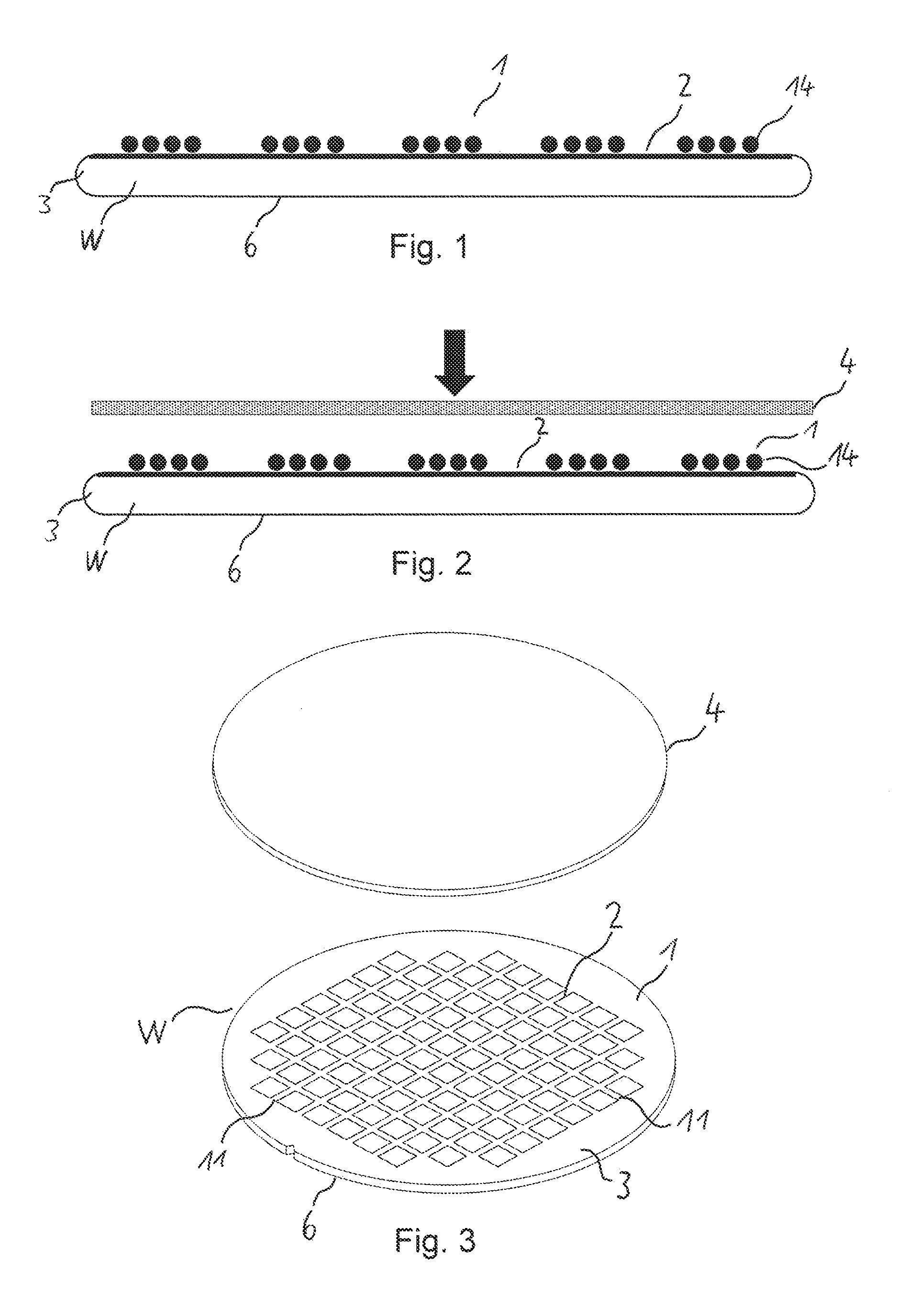
[0080]In the following, a method of processing a wafer W according to the present invention will be described with reference to FIGS. 1 to 13.

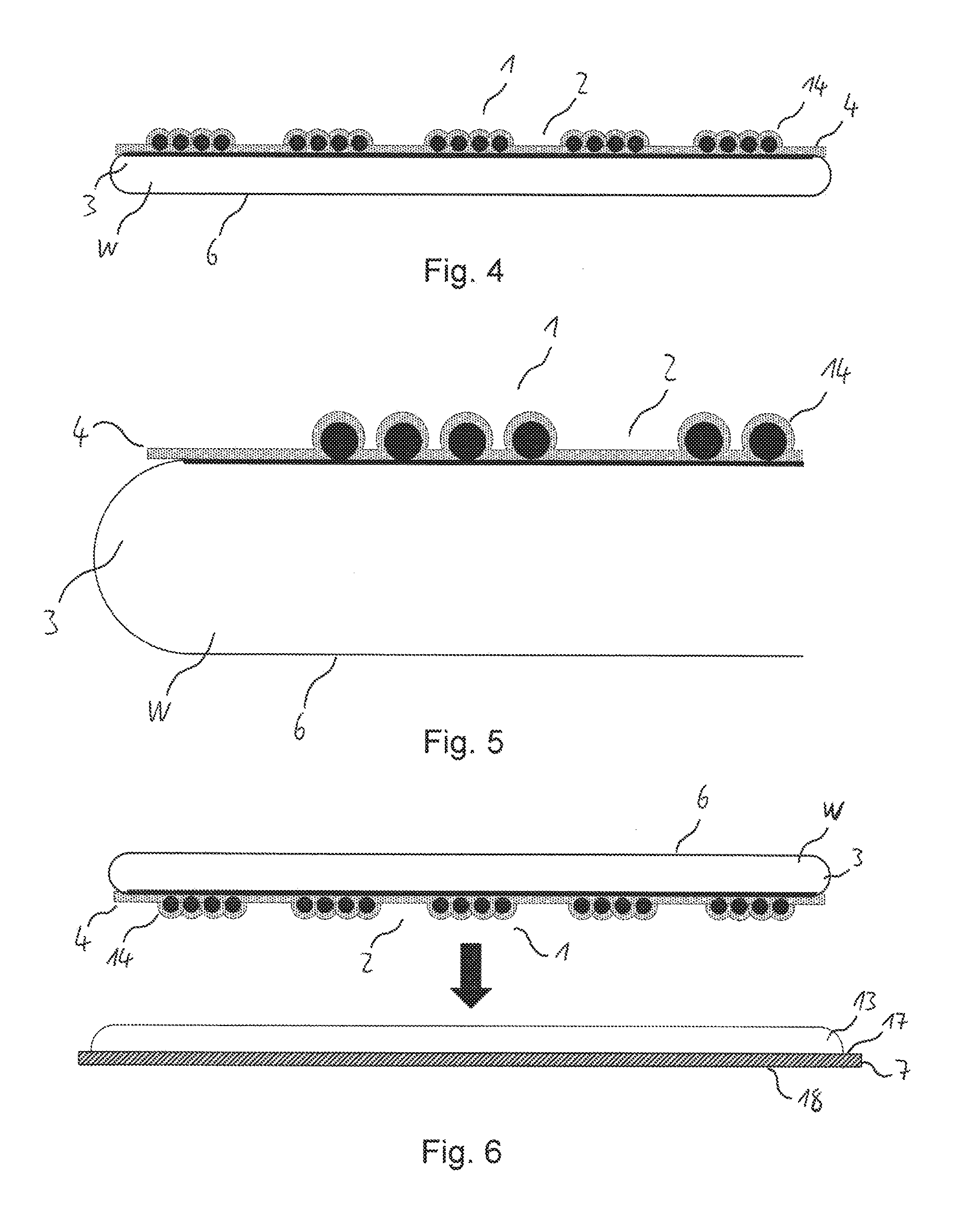
[0081]FIG. 1 shows a cross-sectional view of the wafer W to be processed by the method according to the first embodiment of the present invention. FIGS. 2 and 3 illustrate a first step of the processing method according to this first embodiment. In this first step, a protective film 4, for covering the devices on the wafer W, is attached to the pattern side 1 of the wafer W, as is indicated by an arrow in FIG. 2.

[0082]The protective film 4 preferably has the same shape as the wafer W, i.e., a circular shape in the present embodiment, and is concentrically attached thereto. The diameter of the protective film. 4 is approximately the same as that of the wafer W, as is schematically shown in FIGS. 2 and 3.

[0083]The protective film 4 covers the devices formed in the device area 2, including the protrusions 14, thus protecting the devices against d...

second embodiment

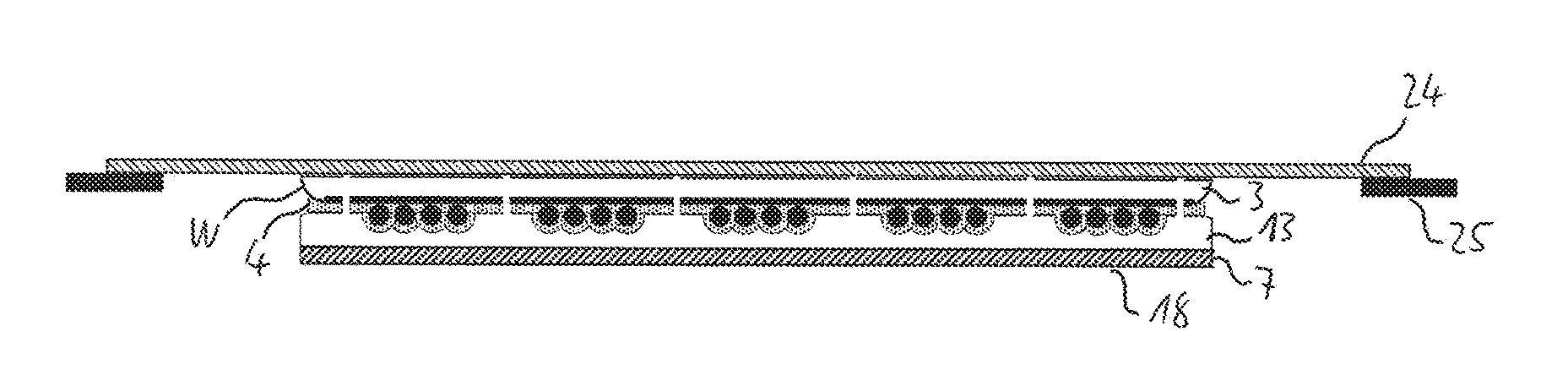
[0116]Specifically, as the sixth step in the method of the second embodiment, cutting of the wafer W is performed in a state in which the protective film 4, the cured resin 13 and the carrier 7 are attached to the wafer W, as is indicated by dashed lines in FIG. 14.

[0117]As is schematically shown in FIG. 14, this cutting process is performed from the ground back side surface of the wafer W. In this cutting process, the back surface 18 of the carrier 7 is placed on the top surface of a chuck table (not shown) which may be identical to the chuck table 20 shown in FIG. 7. Since the protrusions 14 are embedded in the cured resin 13 and the back surface 18 of the carrier 7 is supported by the top surface of the chuck table, the risk of any damage to the wafer W or the dies 26, such as breakage thereof, during cutting is minimised. The wafer W may be cut by mechanical cutting, e.g., using a blade or a saw, and / or cutting by laser and / or cutting by plasma.

[0118]By cutting the wafer W in th...


PUM


Abstract

The invention relates to a method of processing a wafer, having on one side a device area with a plurality of devices partitioned by a plurality of division lines and a peripheral marginal area having no devices and being formed around the device area, wherein the device area is formed with a plurality of protrusions protruding from a plane surface of the wafer. The method comprises attaching a protective film, for covering the devices on the wafer, to the one side of the wafer, wherein the protective film is adhered to at least a part of the one side of the wafer with an adhesive, and providing a carrier having a curable resin applied to a front surface thereof. The method further comprises attaching the one side of the wafer, having the protective film attached thereto, to the front surface of the carrier, so that the protrusions protruding from the plane surface of the wafer are embedded in the curable resin and a back surface of the carrier opposite to the front surface thereof is substantially parallel to the side of the wafer being opposite to the one side, and grinding the side of the wafer being opposite to the one side for adjusting the wafer thickness.

Description

TECHNICAL FIELD[0001]The present invention relates to a method of processing a wafer, such as a semiconductor wafer, having on one side a device area with a plurality of devices partitioned by a plurality of division lines and a peripheral marginal area having no devices and being formed around the device area, wherein the device area is formed with a plurality of protrusions protruding from a plane surface of the wafer.TECHNICAL BACKGROUND[0002]In a semiconductor device fabrication process, a wafer having a device area with a plurality of devices partitioned by a plurality of division lines is divided into individual dies. This fabrication process generally comprises a grinding step for adjusting the wafer thickness and a cutting step of cutting the wafer along the division lines to obtain the individual dies. The grinding step is performed from a back side of the wafer which is opposite to a wafer front side on which the device area is formed.[0003]In known semiconductor device fa...

Claims


Application Information

Patent Timeline
IPC IPC(8): H01L21/78H01L21/56
CPCH01L21/568H01L21/78H01L21/304H01L21/6835H01L2221/68327B81C1/00825B81C1/00896B81C2201/053H01L21/6836H01L24/11H01L24/13H01L2221/68318H01L2221/6834H01L2221/68381H01L2224/11009H01L2224/13014H01L2224/94H01L2924/00014H01L2924/10253H01L2924/12041H01L2924/14H01L2924/1461H01L2224/03H01L2224/11H01L2924/00012H01L2224/13099H01L21/02013H01L21/56H01L21/67092H01L21/76H01L24/00H01L24/94
Inventor PRIEWASSER, KARL HEINZ
Owner DISCO CORP
Why Eureka
Try Eureka