Semiconductor assembly with electromagnetic shielding and thermally enhanced characteristics and method of making the same

a technology of electromagnetic shielding and semiconductors, applied in the direction of semiconductor devices, semiconductor/solid-state device details, electrical apparatus, etc., can solve the problems of inconvenient assembly, immediate failure of operation, and thermal environment of the device, and achieve the effect of effective emi shielding

Active Publication Date: 2017-03-02
BRIDGE SEMICON
View PDF6 Cites 25 Cited by
  • Summary
  • Abstract
  • Description
  • Claims
  • Application Information

AI Technical Summary

Benefits of technology

[0011]The semiconductor assembly and the method of making the same according to the present invention have numerous advantages. For instance, face-to-face electrically coupling the encapsulated device and the thermally enhanced device can offer the shortest interconnect distance between the encapsulated device and the thermally enhanced device. Additionally, inserting the second semiconductor chip into the through opening of the secon

Problems solved by technology

However, as semiconductor devices are susceptible to performance degradation at high operational temperatures, stacking chips with face-to-face configuration without proper heat dissipation would worsen devices' thermal environment and may cause immediate failure during operation.
Since the bottom chip is not protected and has to be

Method used


Image

  • Semiconductor assembly with electromagnetic shielding and thermally enhanced characteristics and method of making the same
  • Semiconductor assembly with electromagnetic shielding and thermally enhanced characteristics and method of making the same
  • Semiconductor assembly with electromagnetic shielding and thermally enhanced characteristics and method of making the same

Examples


embodiment 1

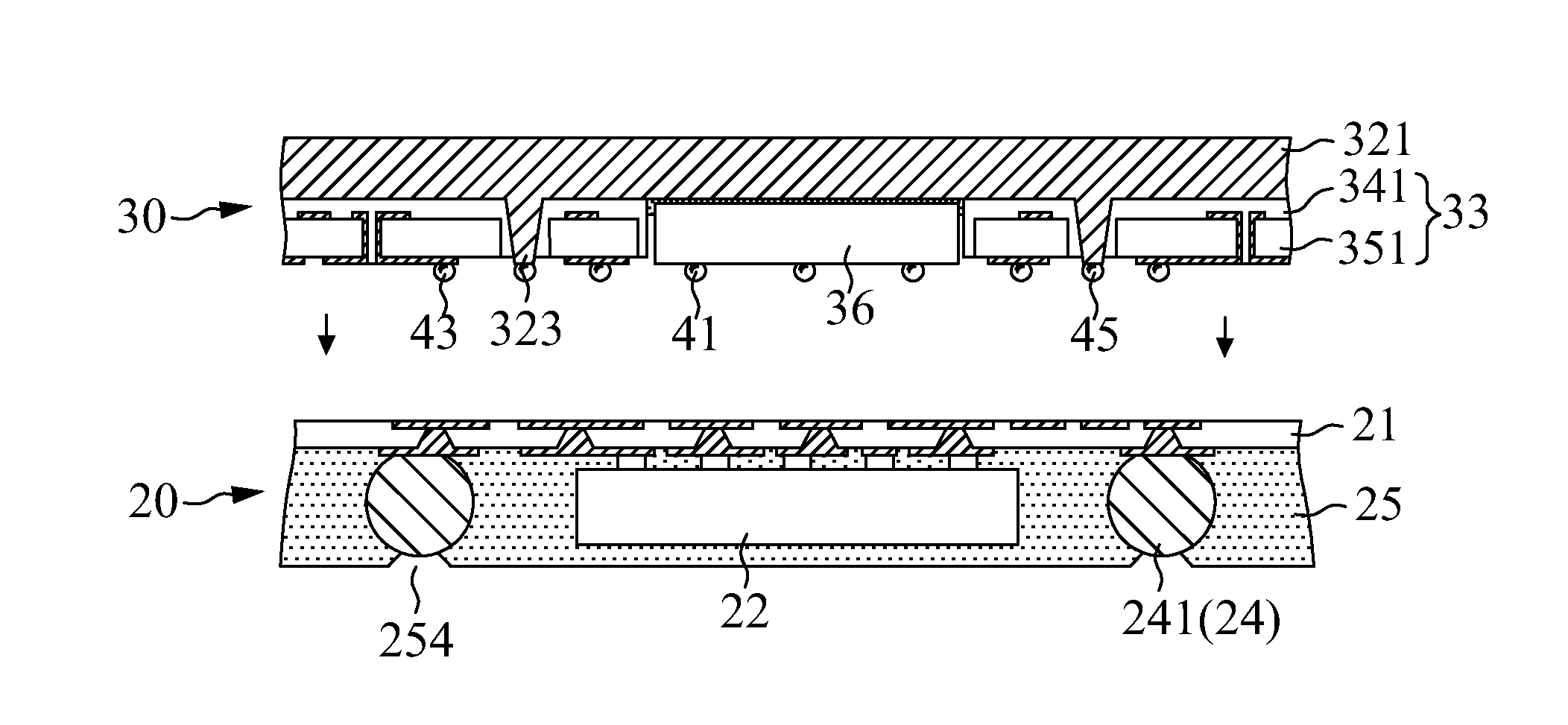
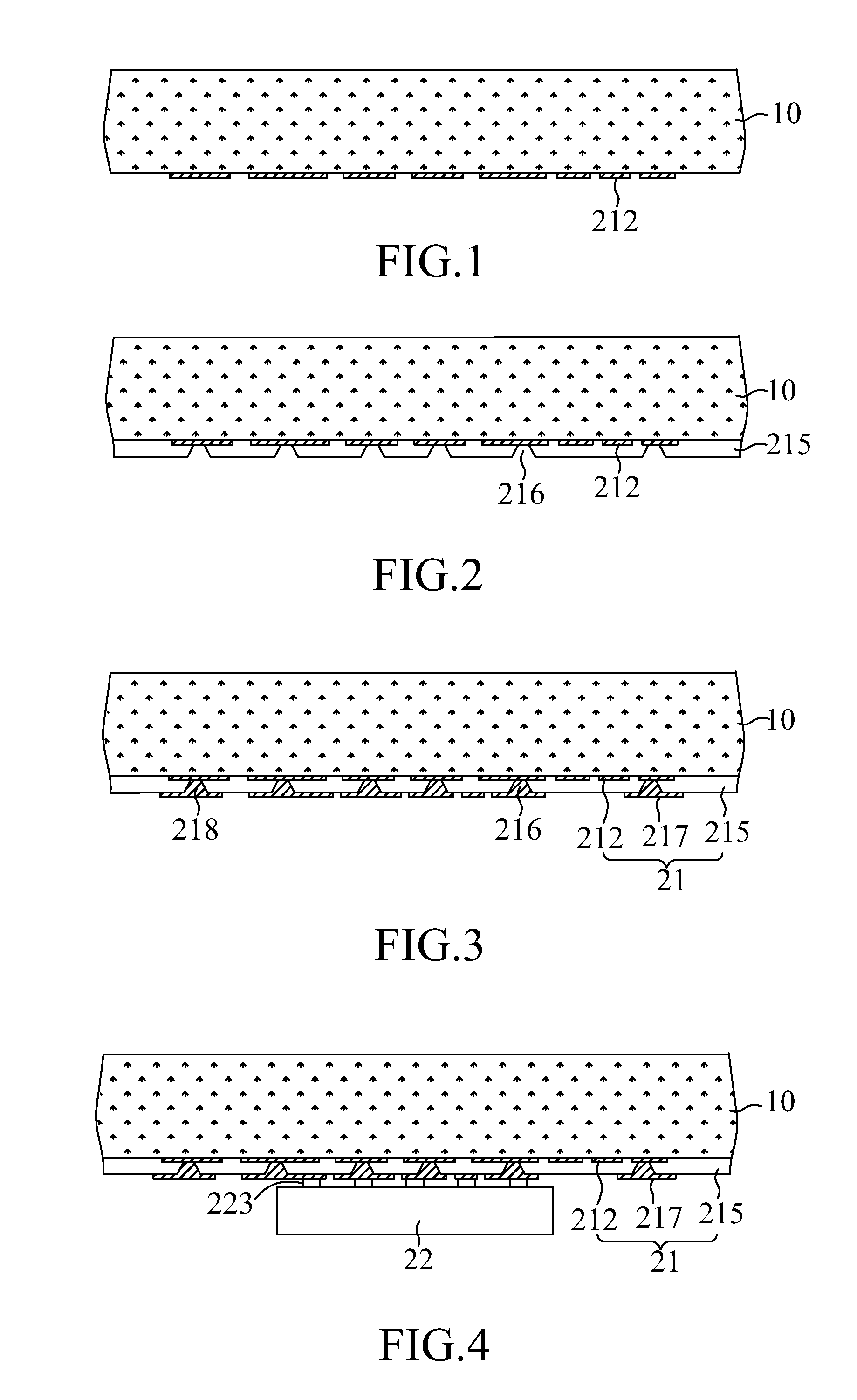
[0079]FIGS. 1-20 are schematic views showing a method of making a semiconductor assembly that includes a first routing circuitry 21, a first semiconductor chip 22, an array of terminals 24, an encapsulant 25, a heat spreader 31 and a second semiconductor chip 36 in accordance with the first embodiment of the present invention.

[0080]FIG. 1 is a cross-sectional view of the structure with routing traces 212 formed on a sacrificial carrier 10 by metal deposition and metal patterning process. In this illustration, the sacrificial carrier 10 is a single-layer structure. The sacrificial carrier 10 typically is made of copper, aluminum, iron, nickel, tin, stainless steel, silicon, or other metals or alloys, but any other conductive or non-conductive material also may be used. In this embodiment, the sacrificial carrier 10 is made of an iron-based material. The routing traces 212 typically are made of copper and can be pattern deposited by numerous techniques, such as electroplating, electro...

embodiment 2

[0107]FIGS. 23-31 are schematic views showing a method of making a semiconductor assembly with an external routing circuitry on the encapsulant in accordance with the second embodiment of the present invention.

[0108]For purposes of brevity, any description in Embodiment 1 above is incorporated herein insofar as the same is applicable, and the same description need not be repeated.

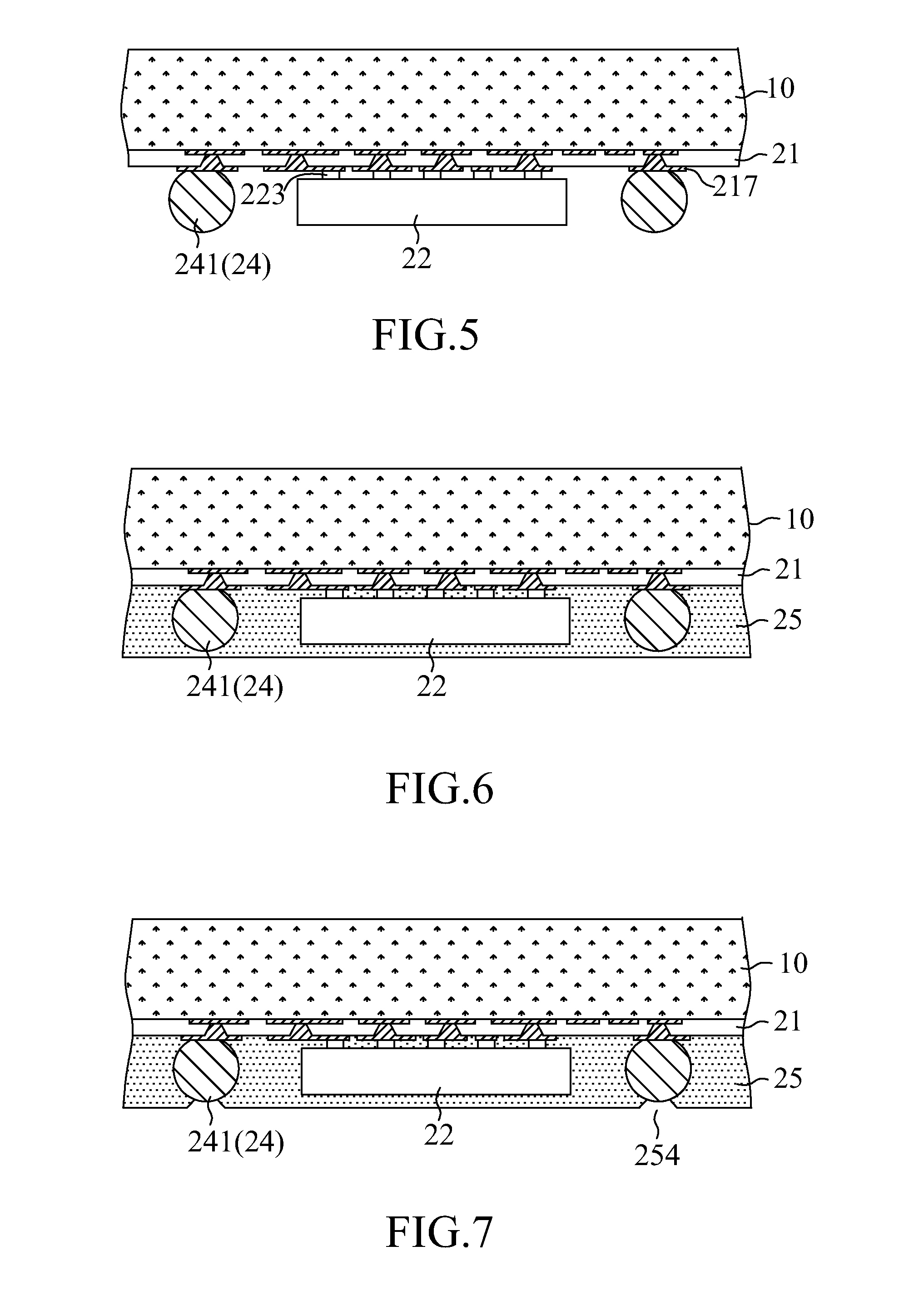
[0109]FIG. 23 is a cross-sectional view of the structure with an encapsulant 25 on the first routing circuitry 21 and the first semiconductor chip 22 of FIG. 4. The encapsulant 25 covers the first routing circuitry 21 and the first semiconductor chip 22 from below and surrounds and conformally coats and covers sidewalls of the first semiconductor chip 22.

[0110]FIG. 24 is a cross-sectional view of the structure with via openings 256 in the encapsulant 25. The via openings 256 are aligned with selected portions of the first conductive traces 217 of the first routing circuitry 21 and extend through the encapsu...

embodiment 3

[0121]FIGS. 34-55 are schematic views showing a method of making a semiconductor assembly with the heat spreader laterally extending beyond peripheral edges of the encapsulated device in accordance with the third embodiment of the present invention.

[0122]For purposes of brevity, any description in Embodiments above is incorporated herein insofar as the same is applicable, and the same description need not be repeated.

[0123]FIGS. 34 and 35 are cross-sectional and top perspective views, respectively, of the structure with multiple sets of alignment guides 28 on a heat spreader 23. The thickness of the heat spreader 23 preferably ranges from 0.1 to 1.0 mm. The alignment guides 28 project from a surface of the heat spreader 23 and can have a thickness of 5 to 200 microns. In this embodiment, the heat spreader 23 has a thickness of 0.5 mm, whereas the alignment guides 28 have a thickness of 50 microns. The alignment guides 28 can be pattern deposited by numerous techniques, such as elect...


PUM


Abstract

A semiconductor assembly includes an encapsulated device and a thermally enhanced device face-to-face mounted together through first and second routing circuitries and a heat spreader that provides thermal dissipation and electromagnetic shielding. The encapsulated device has a first semiconductor chip sealed in an encapsulant, whereas the thermally enhanced device has a second semiconductor chip thermally conductible to a shielding lid of the heat spreader and laterally surrounded by posts of the heat spreader. The first and second semiconductor chips are mounted on two opposite sides of the first routing circuitry, and the second routing circuitry is disposed on the shielding lid and electrically coupled to the first routing circuitry by bumps. The first and second routing circuitries provide staged fan-out routing for the first and second semiconductor chips.

Description

CROSS REFERENCE TO RELATED APPLICATIONS[0001]This application is a continuation-in-part of U.S. application Ser. No. 15 / 166,185 filed May 26, 2016 and continuation-in-part of U.S. application Ser. No. 15 / 289,126 filed Oct. 8, 2016. The U.S. application Ser. No. 15 / 166,185 claims the priority benefit of U.S. Provisional Application Ser. No. 62 / 166,771 filed May 27, 2015. The entirety of each of said applications is incorporated herein by reference.FIELD OF THE INVENTION[0002]The present invention relates to a semiconductor assembly and, more particularly, to a semiconductor assembly in which two semiconductor devices are face-to-face mounted together through dual routing circuitries and a heat spreader provides thermal dissipation and electromagnetic shielding, and a method of making the same.DESCRIPTION OF RELATED ART[0003]Market trends of multimedia devices demand for faster and slimmer designs. One of assembly approaches is to interconnect two semiconductor devices with “face-to-f...

Claims


Application Information

Patent Timeline
IPC IPC(8): H01L25/10H01L23/373H01L25/00H01L23/538H01L23/498H01L23/552H01L23/367
CPCH01L25/105H01L23/552H01L23/3736H01L23/3675H01L23/5389H01L2225/1094H01L23/49816H01L25/50H01L2225/1035H01L2225/1058H01L2225/107H01L23/49838H01L2924/37001H01L2224/83005H01L23/13H01L23/16H01L23/3128H01L23/36H01L23/49822H01L21/561H01L21/568H01L23/544H01L24/16H01L24/19H01L24/20H01L24/32H01L21/6835H01L24/73H01L24/81H01L24/83H01L24/92H01L24/97H01L25/0657H01L2221/68359H01L2221/68381H01L2223/54426H01L2223/54486H01L2224/04105H01L2224/12105H01L2224/16227H01L2224/16235H01L2224/32225H01L2224/32245H01L2224/73253H01L2224/73267H01L2224/81005H01L2224/81203H01L2224/81207H01L2224/81815H01L2224/8314H01L2224/92225H01L2224/92244H01L2224/97H01L2225/0651H01L2225/06589H01L2924/15153H01L2924/15311H01L2924/3025H01L2924/3511H01L2225/06572H01L2225/06537H01L2224/83132H01L23/3135H01L23/5385H01L25/03H01L25/0652H01L2224/32145H01L2224/48091H01L2224/48227H01L2224/48235H01L2224/73204H01L2224/73265H01L2225/06517H01L2924/15313H01L2924/15321H01L2924/1533H01L2924/18161H01L2225/06562H01L2225/06548H01L2224/83H01L2224/81H01L2924/00012H01L2924/00014H01L2924/00H01L2224/16225
Inventor LIN, CHARLES W. C.WANG, CHIA-CHUNG
Owner BRIDGE SEMICON
Why Eureka
Try Eureka