

Processing of superhydrophobic, infrared transmissive, Anti-reflective nanostructured surfaces
a nanostructured surface, infrared transmissive technology, applied in the field of making superhydrophobic materials, can solve problems such as increasing the hydrophilicity of materials
- Summary
- Abstract
- Description
- Claims
- Application Information
AI Technical Summary
Benefits of technology
Problems solved by technology
Method used
Image

Examples
example 1
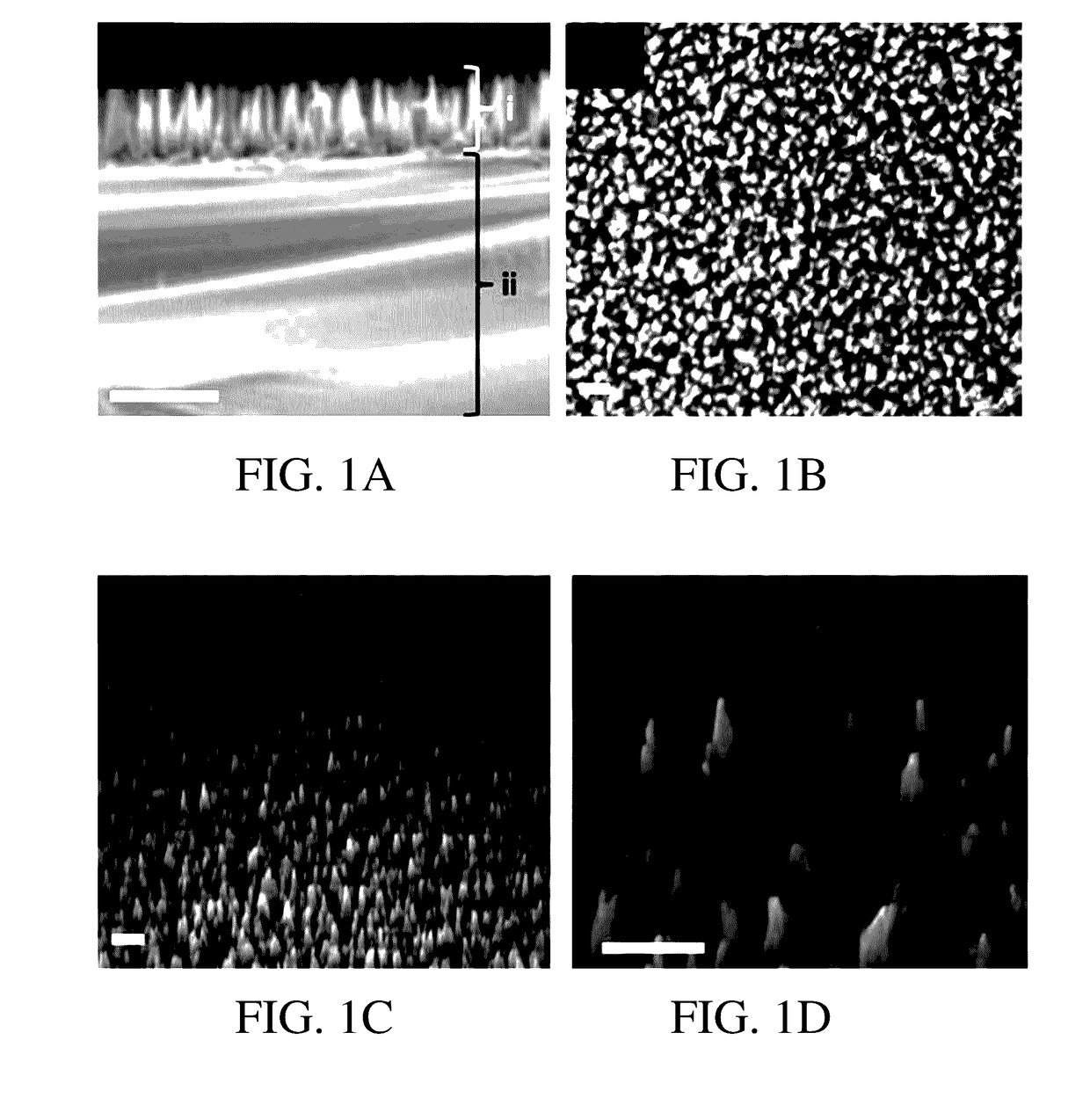
[0067]UV grade fused-silica substrates, which were randomly pre-patterned on one side with nanostructures extending approximately 800 nm into the surface of the substrate, were subjected to an O2(g) atmosphere for 10 minutes in a March Plasma Reactive Ion Etcher under a pressure of 320 mTorr, and at a power of 200 W. The substrates were then removed, immersed and swirled for 30 seconds in hexanes that contained 0.5% 1H,1H,2H,2H-perfluorooctyl trichlorosilane (PFOTS). The substrates were immediately rinsed with hexanes, blown dry with N2(g) and placed in an oven to bake for 15 minutes at 120° C. The substrates were removed from the oven and allowed to cool.
Water Contact Angle Analysis
[0068]Water contact angle measurements were taken using the devices of Comparative Examples 1-3 and Example 1. The device of Comparative Example 1 had a contact angle indicative of a hydrophilic substance. The contact angle of the device of Comparative Example 3 was found to be nearly 0° (i.e. superhydro...
example 2
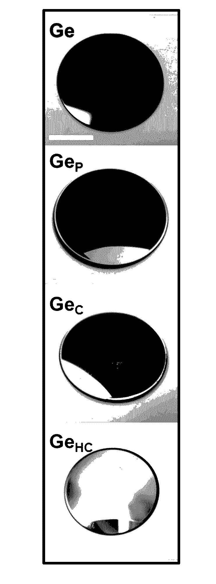
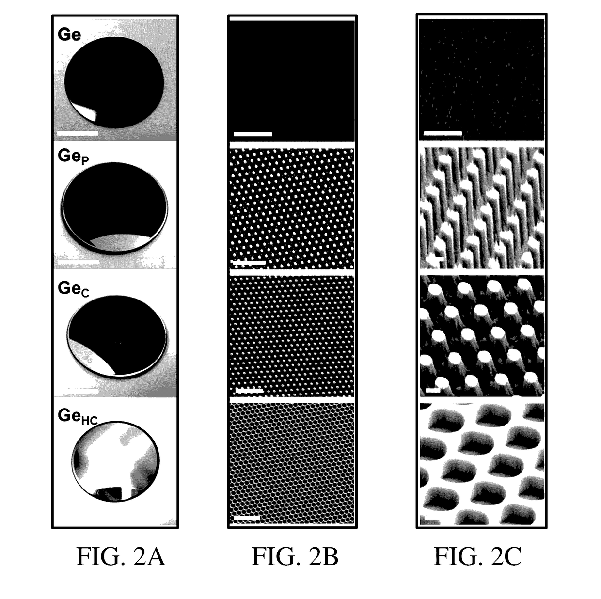
[0082]PFOTS (or similar functioning species) can be applied to other optical materials with surface anti-reflective structures to enable superhydrophobicity in other wavelength regions, such as the mid-wave infrared (MWIR) and long-wave infrared (LWIR). The application to substrate materials other than fused silica was demonstrated in Example 2 using germanium substrates. Each device using a germanium substrate had a differently shaped periodic, nanoscale surface pattern as shown in FIG. 2A, FIG. 2B, and FIG. 2C. These non-random patterns include nano-pillars (shown as GeP), truncated nano-cones (shown as GeC), and / or honeycomb patterns (shown as GeHC). The substrates were chemically treated using the same process as described in Example 1.
Water Contact Angle Analysis
[0083]Following chemical modification of the germanium substrates, the contact angle for water was measured following the procedure included above. After chemical modification with PFTOS, each of the germanium substrate...
PUM
| Property | Measurement | Unit |
|---|---|---|
| temperature | aaaaa | aaaaa |
| contact angle | aaaaa | aaaaa |
| contact angle | aaaaa | aaaaa |
Abstract
Description
Claims
Application Information