Capacitive-coupled non-volatile thin-film transistor strings in three dimensional arrays

a capacitor-coupled, non-volatile technology, applied in the direction of digital storage, solid-state devices, instruments, etc., can solve the problems of long latency, limiting the number of transistors that can be programmed in parallel, and unread active tfts that are not read or programmed may experience undesirable program-disturb or read-disturb conditions, etc., to achieve reduced read-latency, reduced sensitivities, and greater storage density

Active Publication Date: 2017-03-30
SUNRISE MEMORY CORP
View PDF4 Cites 266 Cited by
  • Summary
  • Abstract
  • Description
  • Claims
  • Application Information

AI Technical Summary

Benefits of technology

[0020]In one embodiment, TFTs are formed using both vertical side edges of each active strip, with vertical local word lines being provided along both the vertical side edges of the active strips. In that embodiment, double-density is achieved by having the local word lines along one of vertical edges of an active strip contacted by horizontal global word lines provided above the active strip, while the local word lines along the other vertical edge of the active strip are contacted by horizontal global word lines provided beneath the active strip. All global word lines may run in a direction transverse to the direction along the lengths of the corresponding active strips. Even greater storage density may be achieved by storing more than one bit of data in each TFT.
[0021]Organizing the TFTs into NOR strings in the memory array—rather than the prior art NAND strings—results in (i) a reduced read-latency that approaches that of a dynamic random access memory (DRAM) array, (ii) reduced sensitivities to read-disturb and program-disturb conditions that are known to be associated with long NAND strings, (iii) reduced power dissipation and a lower cost-per-bit relative to planar NAND or 3-D NAND arrays, and (iv) the ability to read, write or erase TFTs on multiple active strips concurrently to increase data throughput.
[0022]Accordi

Problems solved by technology

Under this NAND arrangement, the activated TFTs that are not read or programmed may experience undesirable program-disturb or read-disturb conditions.
The low read current that is required to be conducted through a long NAND string results in a long latency.
Channel hot-electron injection programming requires a relatively large electron current to f

Method used


Image

  • Capacitive-coupled non-volatile thin-film transistor strings in three dimensional arrays
  • Capacitive-coupled non-volatile thin-film transistor strings in three dimensional arrays
  • Capacitive-coupled non-volatile thin-film transistor strings in three dimensional arrays

Examples


embodimentd

Some Specific Embodimentd of the Present Invention

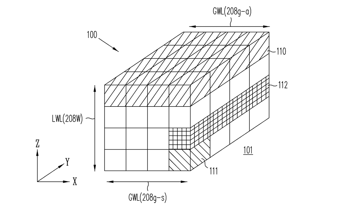
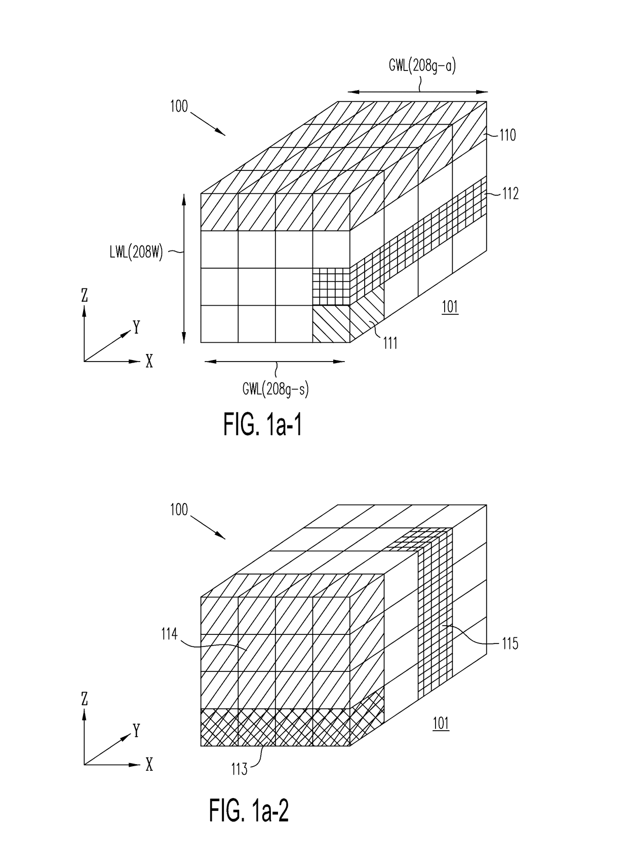
[0108]In embodiment EMB-1, shown in FIGS. 2i and 4a, each of local word lines 208W is connected to either one of global word lines 208a-a (routed in one or more layers provided above active layers 202-0 to 202-7), or one of global word lines 208g-s (routed in one or more layers provided below the active layers between active layer 202-0 and substrate 201). Local word lines 208W-s that are coupled to bottom global word lines 208g-s may be assigned odd addresses, while local word lines 208W-a coupled to the top global word lines 208a-a may be assigned even addresses, or vice versa. FIG. 4a is a cross section in the X-Y plane of embodiment EMB-1 of FIGS. 2i and 2i-1, showing contacts 291 connecting local word lines 208W-a to global word lines 208a-a at the top of the memory array. Likewise, local word lines 208W-s are connected to global word lines 208g-s (not shown) running at the bottom of the memory array substantially parallel to th...


PUM


Abstract

Multi-gate NOR flash thin-film transistor (TFT) string arrays are organized as three dimensional stacks of active strips. Each active strip includes a shared source sublayer and a shared drain sublayer that is connected to substrate circuits. Data storage in the active strip is provided by charge-storage elements between the active strip and a multiplicity of control gates provided by adjacent local word-lines. The parasitic capacitance of each active strip is used to eliminate hard-wire ground connection to the shared source making it a semi-floating, or virtual source. Pre-charge voltages temporarily supplied from the substrate through a single port per active strip provide the appropriate voltages on the source and drain required during read, program, program-inhibit and erase operations. TFTs on multiple active strips can be pre-charged separately and then read, programmed or erased together in a massively parallel operation.

Description

CROSS REFERENCE TO RELATED APPLICATIONS[0001]The present invention is related to and claims priority of (i) copending U.S. provisional application (“Copending Provisional Application I”), Ser. No. 62 / 235,322, entitled “Multi-gate NOR Flash Thin-film Transistor Strings Arranged in Stacked Horizontal Active Strips With Vertical Control Gates,” filed on September 30, 2015; (ii) U.S. provisional patent application (“Copending Provisional Application II”), Ser. No. 62 / 260,137, entitled “Three-dimensional Vertical NOR Flash Thin-film Transistor Strings,” filed on November 25, 2015; (iii) U.S. non-provisional patent application (“Copending Non-Provisional Application”) to which this application is a continuation-in-part of, Ser. No. 15 / 220,375, “Multi-Gate NOR Flash Thin-film Transistor Strings Arranged in Stacked Horizontal Active Strips With Vertical Control Gates,” filed on Jul. 26, 2016; and (vi) copending U.S. provisional patent application (“Copending Provisional Application III”), S...

Claims


Application Information

Patent Timeline
IPC IPC(8): G11C16/34G11C11/56H01L29/92H01L29/10H01L29/08H01L29/786G11C16/04H01L27/115
CPCG11C16/3431H01L29/7923G11C11/5628G11C11/5635G11C11/5642G11C16/0483H01L27/115H01L29/1037H01L29/0847H01L29/78633H01L29/92H01L27/11556H01L27/11521H01L27/11582H01L27/11568H01L29/7883G11C16/0466G11C16/0416G11C16/0491H01L29/66833H01L29/7926H01L29/40117H10B43/10H10B43/27G11C16/10
Inventor HARARI, ELI
Owner SUNRISE MEMORY CORP
Why Eureka
Try Eureka