Conductive Polymer Dispersion with Enhanced Coverage

Active Publication Date: 2017-04-06
KEMET ELECTRONICS
View PDF17 Cites 5 Cited by
  • Summary
  • Abstract
  • Description
  • Claims
  • Application Information

AI Technical Summary

Benefits of technology

[0014]U.S. Pat. No. 9,030,807, which is incorporated herein by reference, teaches a method for avoiding crosslinking of ionic compounds as well as for improving the coverage by

Problems solved by technology

In the doped state, the polymer is conductive but of poor processibility due to a high degree of conjugation along the polymer chain.
The major drawback of conductive polymer capacitors, regardless of the types of conductive polymers employed, is their relatively low working voltage compared to their MnO2 counterparts.
The polymer capacitors have reliability issues, to varying degrees, when the voltage rating exceeds 25V.
This is believed to be caused by the relatively poor dielectric-polymer interface, which has poor “self-healing” capability.
This limitation has thwarted efforts to use conductive polymers more extensively.
However, it is a challenge to form a conductive polymer coating on the anodes that is defect-free, and which is capable of withstanding thermal mechanical stress during anode resin encapsulation and surface-mounting.
The improper application of polymer slurry often leads to the formation of a poor polymer coating.
These materials tend to pull away from the corner

Method used


Image

  • Conductive Polymer Dispersion with Enhanced Coverage
  • Conductive Polymer Dispersion with Enhanced Coverage
  • Conductive Polymer Dispersion with Enhanced Coverage

Examples


Example

Comparative Example 1

[0056]A series of D case 33 μF, 35V tantalum anodes was prepared. A thin coating of polyethylenedioxythiophene polymer (PEDOT) was applied on the dielectric of the anodes via an in-situ chemical polymerization process to achieve full capacitance. The anodes were then coated with conductive polymer dispersion. The conductive polymer dispersion coating was repeated 4 more times. The cured parts were analyzed by an Scanning Electron Microscope (SEM) for polymer coverage and a percentage coverage was obtained. Representations of the SEM micrographs are provided in FIGS. 1 and 2. Graphite and Ag coatings were applied and the samples electrical properties were analyzed. The coverage and electrical properties are recorded in Table 1.

Example

Comparative Example 2

[0057]A series of D case 33 μF, 35V tantalum anodes were prepared. A thin coating of conductive polymer (PEDOT) was applied onto the anodes via an in-situ chemical polymerization process. The anodes were first coated with conductive polymer dispersion. After drying, alternating layers of a commercial crosslinker (Clevios K primer) and the conductive polymer dispersion were applied and repeated 3 more times followed by curing. The cured parts were analyzed by SEM for polymer coverage and a percentage coverage was obtained. Representations of the SEM images are provided in FIGS. 3 and 4. Graphite and Ag coatings were applied and the samples electrical properties were analyzed. The coverage and electrical properties are recorded in Table 1.

Example

Inventive Example 1

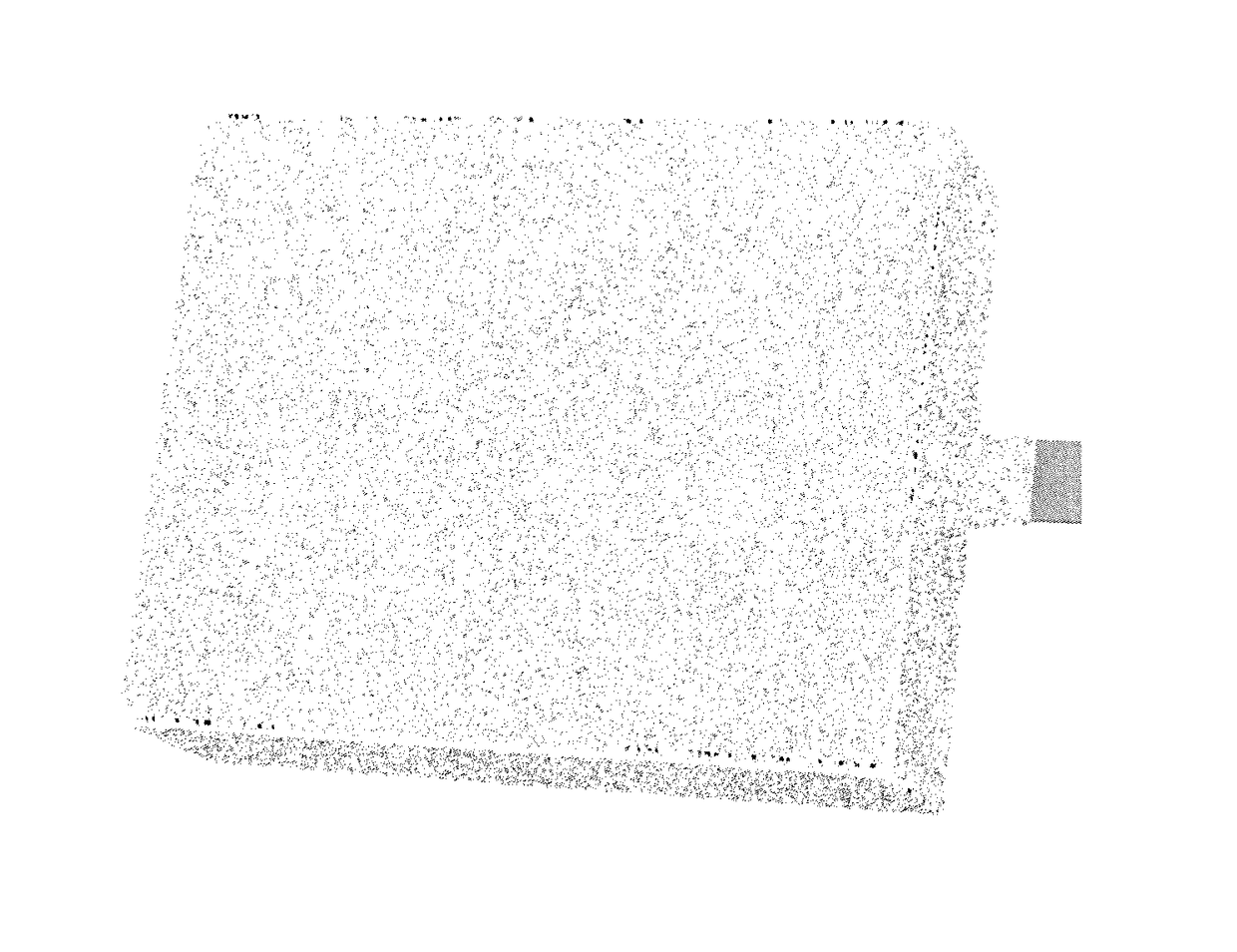
[0058]A series of D case 33 μF, 35V tantalum anodes were prepared. A thin coating of conductive polymer (PEDOT) was applied onto the anodes via an in-situ chemical polymerization process. The anodes were first coated with a conductive polymer dispersion. A conducting polymer dispersion comprising amine compounds was prepared. After drying a conductive polymer dispersion comprising amine compounds was applied over the first conducting polymer dispersion. The conductive polymer dispersion comprising amine compounds was applied 3 more times followed by curing. The cured parts were analyzed by SEM for polymer coverage and a percentage coverage was obtained. Representations of the SEM images are provided in FIGS. 5 and 6. Graphite and Ag coatings were applied and the samples electrical properties were analyzed. The coverage and electrical properties are recorded in Table 1.

TABLE 1Comparison of bias HAST ESR shift for prior art and inventiveExamplesPolymer CoverageESR (...


PUM

PropertyMeasurementUnit
Fractionaaaaaaaaaa
Fractionaaaaaaaaaa
Fractionaaaaaaaaaa

Abstract

An improved process for forming an electrolytic capacitor is provided. The process comprises: providing an anode with an anode wire extending from the anode body; forming a dielectric on the anode to form an anodized anode; applying a first slurry wherein the first slurry comprises conducting polymer and polyanion, wherein the polyanion and conducting polymer are in a first weight ratio thereby forming a first slurry layer; and applying a second slurry on the first slurry layer wherein the second slurry comprises the conducting polymer and said polyanion and wherein the polyanion and the conducting polymer are in a second weight ratio wherein the second weight ratio is lower than the first weight ratio.

Description

CROSS-REFERENCE TO RELATED APPLICATIONS[0001]The present application claims priority to pending U.S. Pat. Appl. No. 62 / 267,707 filed Dec. 15, 2015. The present invention is a continuation-in-part application of pending U.S. patent application Ser. No. 14,743,195 filed Jun. 18, 2015 which is, in turn, a continuation-in-part application of U.S. patent application Ser. No. 13 / 777,769 filed Feb. 26, 2013 now U.S. Pat. No. 9,312,074 issued Apr. 12, 2016, which in turn, claims priority to expired U.S. Provisional Patent Appl. No. 61 / 603,635 filed Feb. 26, 2012 all of which are incorporated herein by reference.BACKGROUND[0002]The present invention is related to an improved method of forming a solid electrolytic capacitor and an improved capacitor formed thereby. More specifically, the present invention is related to materials and methods for improving corner and edge coverage of solid electrolytic capacitors. The invention also discloses methods for manufacturing the same.[0003]The constru...

Claims


Application Information

Patent Timeline
IPC IPC(8): H01G9/048H01G9/045H01G9/15H01G9/042H01G9/00H01G9/025
CPCH01G9/048H01G9/0036H01G9/045H01G9/15H01G9/042H01G9/025H01G9/012H01G9/028H01G9/0425H01G9/08Y10T29/43
Inventor CHACKO, ANTONY P.LESSNER, PHILLIP M.OLS, JOHN JOSEPHSHI, YARUCHEN, QINGPING
Owner KEMET ELECTRONICS
Why Eureka
Try Eureka