Two-dimensional heterojunction interlayer tunneling field effect transistors

a field effect transistor and heterojunction technology, applied in transistors, semiconductor devices, electrical equipment, etc., can solve the problems of increasing device-to-device variability, power dissipation of such circuits, and power consumption in these integrated circuits

Inactive Publication Date: 2017-04-06
UNIV OF NOTRE DAME DU LAC
View PDF2 Cites 26 Cited by
  • Summary
  • Abstract
  • Description
  • Claims
  • Application Information

AI Technical Summary

Problems solved by technology

However, power dissipation of such circuits has recently become a considerable challenge.
Rates of power consumption in these integrated circuits can affect, for example, the useful lifespan of portable equipment, the sustainability of the ever-increasing number of large data centers, the feasibility of energy-autonomous systems in terms of ambience intelligence, and the feasibility of sensor networks associated with implants and other medical devices, among others.
While the scaling of a supply voltage (VDD) is recognized as one of the most effective measures for reducing switching power in digital circuits, the performance loss and increased device-to-device variability are typically seen as serious hindrances to scaling VDD down to 0.5 volts (V) or less.
Even if encouraging experimental results have been reported for the on-current in group III-V tunnel FETs, achieving a sub-60 mV / dec SS remains a major challenge in these devices, likely due to the detrimental effects of interface states.

Method used


Image

  • Two-dimensional heterojunction interlayer tunneling field effect transistors
  • Two-dimensional heterojunction interlayer tunneling field effect transistors
  • Two-dimensional heterojunction interlayer tunneling field effect transistors

Examples


Embodiment Construction

[0031]The following description of example methods and apparatus is not intended to limit the scope of the description to the precise form or forms detailed herein. Instead the following description is intended to be illustrative so that others may follow its teachings.

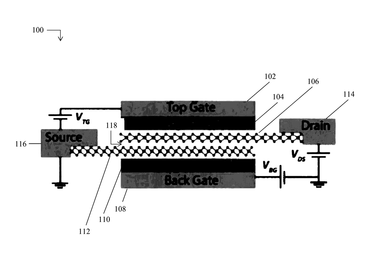
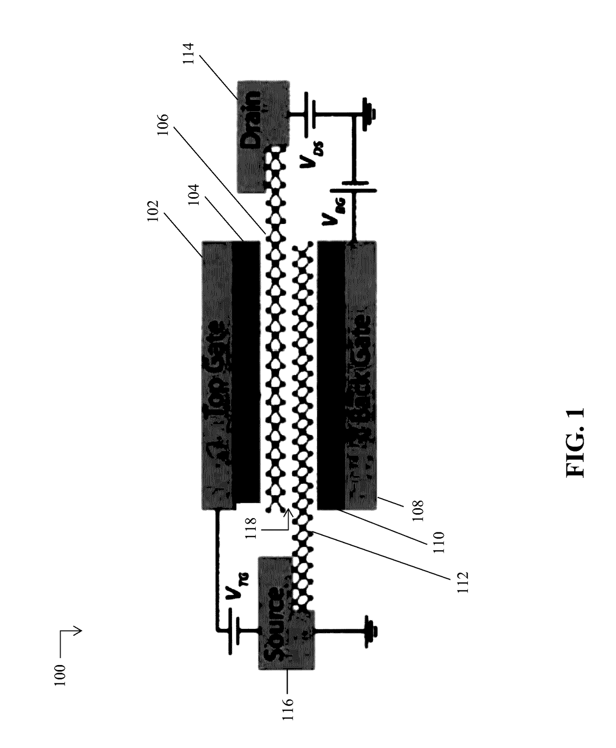
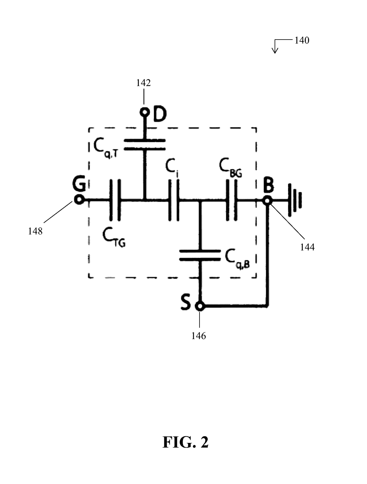
[0032]Monolayers of group-VIB transition metal dichalcogenides (TMDs) according to the formula MX2—where M=Mo or W, and where X=S, Se, or Te—have recently attracted attention for their electronic and optical properties. As explained below, these materials may be utilized by the 2D crystal layers in the example 2D heterojunction interlayer tunneling field effect transistors (Thin-TFETs) disclosed herein. Monolayers of TMDs have a bandgap that varies from almost zero to 2 eV with a sub-nanometer thickness. As a result, these materials are considered to be approximately two-dimensional (2D) crystals. 2D crystals, in turn, have recently attracted attention primarily due to their scalability, step-like density of states, a...


PUM


Abstract

A two-dimensional (2D) heterojunction interlayer tunneling field effect transistor (Thin-TFET) allows for particle tunneling in a vertical stack comprising monolayers of two-dimensional semiconductors separated by an interlayer. In some examples, the two 2D materials may be misaligned so as to influence the magnitude of the tunneling current, but have a modest impact on gate voltage dependence. The Thin-TFET can achieve very steep subthreshold swing, whose lower limit is ultimately set by the band tails in the energy gaps of the 2D materials produced by energy broadening. These qualities in turn make the Thin-TFET an ideal low voltage, low energy solid state electronic switch.

Description

CROSS REFERENCE TO RELATED APPLICATION[0001]This application is a non-provisional application claiming priority from U.S. Provisional Application Ser. No. 62 / 118,980, filed Feb. 20, 2015, entitled “Two-Dimensional Heterojunction Interlayer Tunneling Field Effect Transistors” and incorporated herein by reference in its entirety.GOVERNMENT LICENSE RIGHTS[0002]This invention was made with government support under Contract FA9550-12-1-0257 awarded by the Air Force Office of Scientific Research. The government has certain rights in the invention.FIELD OF THE DISCLOSURE[0003]The present description relates generally to particle tunneling and field effect transistors and, more particularly, to two-dimensional heterojunction interlayer tunneling field effect transistors.BACKGROUND OF RELATED ART[0004]Electronic integrated circuits may be considered the hardware backbone of today's information society. However, power dissipation of such circuits has recently become a considerable challenge. ...

Claims


Application Information

Patent Timeline
Patent Type & Authority Applications(United States)
IPC IPC(8): H01L29/786H01L29/18H01L29/15
CPCH01L29/78648H01L29/18H01L29/151H01L29/7391H01L29/78681H01L29/78696H01L29/045H01L29/24
Inventor LI, MINGDAESSENI, DAVIDSNIDER, GREGORYJENA, DEBDEEPXING, HUILI GRACE
Owner UNIV OF NOTRE DAME DU LAC
Why Eureka
Try Eureka