Method of manufacturing electronic device and composite film

a technology of which is applied in the field of manufacturing electronic devices and composite films, can solve the problems of electronic devices that are not suitable for use, electronic devices that are occasionally deteriorated, and the drying of pressure sensitive adhesive layers cannot be properly performed, so as to achieve stable manufacturing of high-quality electronic devices, prevent foreign matter adhesion, and easy and reliably dry pressure sensitive adhesive layers

Inactive Publication Date: 2017-04-13
FUJIFILM CORP
View PDF6 Cites 8 Cited by
  • Summary
  • Abstract
  • Description
  • Claims
  • Application Information

AI Technical Summary

Benefits of technology

[0020]An object of the present invention is to solve the above-described problems of the related art and to provide a method of manufacturing an electronic device in which deterioration of the electronic device due to moisture can be prevented during the manufacture of the electronic device such as an organic EL device formed by sealing an organic EL device body with a gas barrier film so that an increase in production costs can be suppressed; and a composite film used for this manufacturing method.
[0032]According to the present invention, it is possible to easily and reliably dry a pressure sensitive adhesive layer and to prevent adhesion of foreign matter to the pressure sensitive adhesive layer during the drying when an organic EL device in which an organic EL device body is sealed with a gas barrier film or the like having a pressure sensitive adhesive layer is manufactured. That is, the organic EL device body can be sealed by the composite film which does not have foreign matter adhering thereto and in which the pressure sensitive adhesive layer is reliably dried.
[0033]Therefore, according to the present invention, it is possible to stably manufacture a high-quality electronic device which does not have moisture, foreign matter, deterioration caused by moisture or foreign matter, or defects.

Problems solved by technology
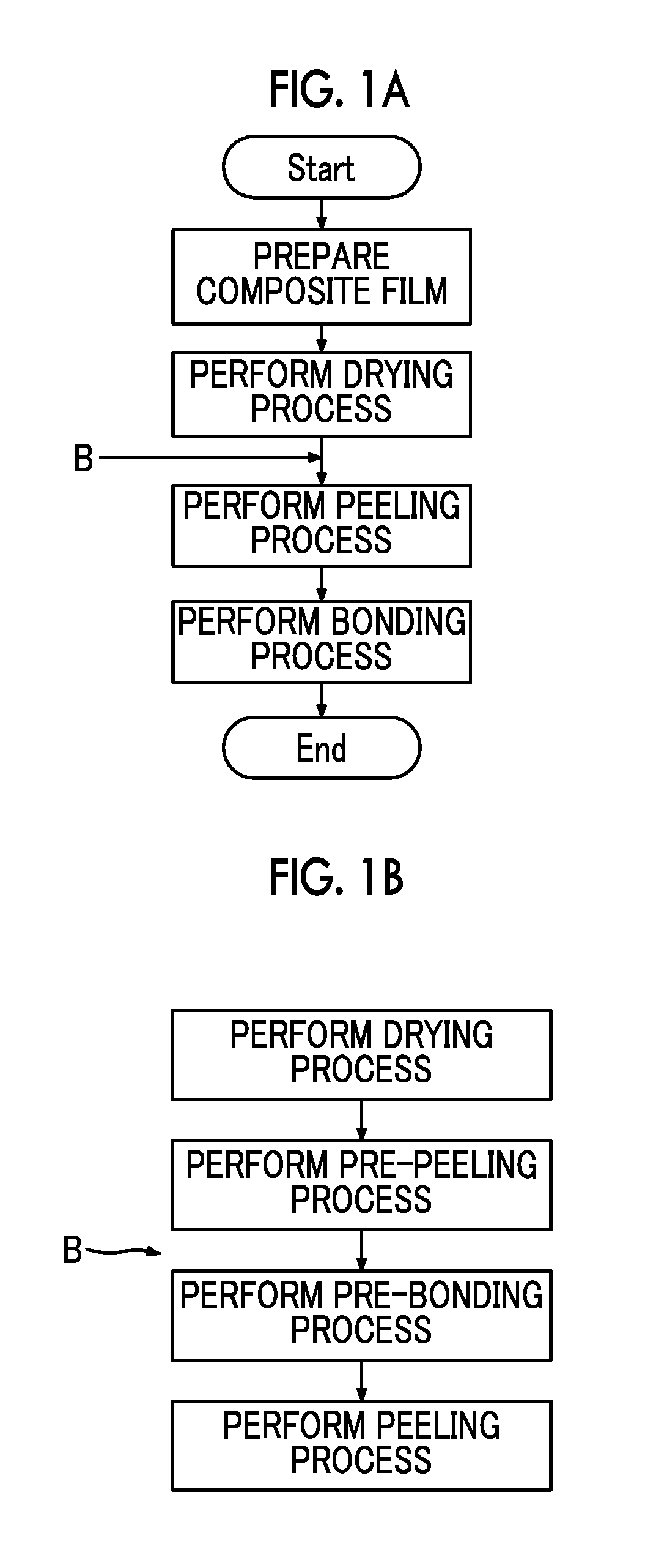
In such a method of manufacturing an electronic device of the related art, when an electronic device having an element deteriorating due to moisture, such as an organic EL device or a solar cell, is manufactured, an electronic device occasionally deteriorates due to the moisture contained in a pressure sensitive adhesive layer.
However, since a protective film or the like is bonded to the pressure sensitive adhesive layer of the composite film when a method of manufacturing an electronic device of the related art is used, drying of the pressure sensitive adhesive layer cannot be properly performed.
However, in this manufacturing method, foreign matter adheres to the pressure sensitive adhesive layer which is exposed during the drying and thus defects or the like may occur in an electronic device due to the foreign matter.
Therefore, the cost of facilities and the production costs increase and the productivity is degraded.

Method used


Image

  • Method of manufacturing electronic device and composite film
  • Method of manufacturing electronic device and composite film
  • Method of manufacturing electronic device and composite film

Examples


example 1

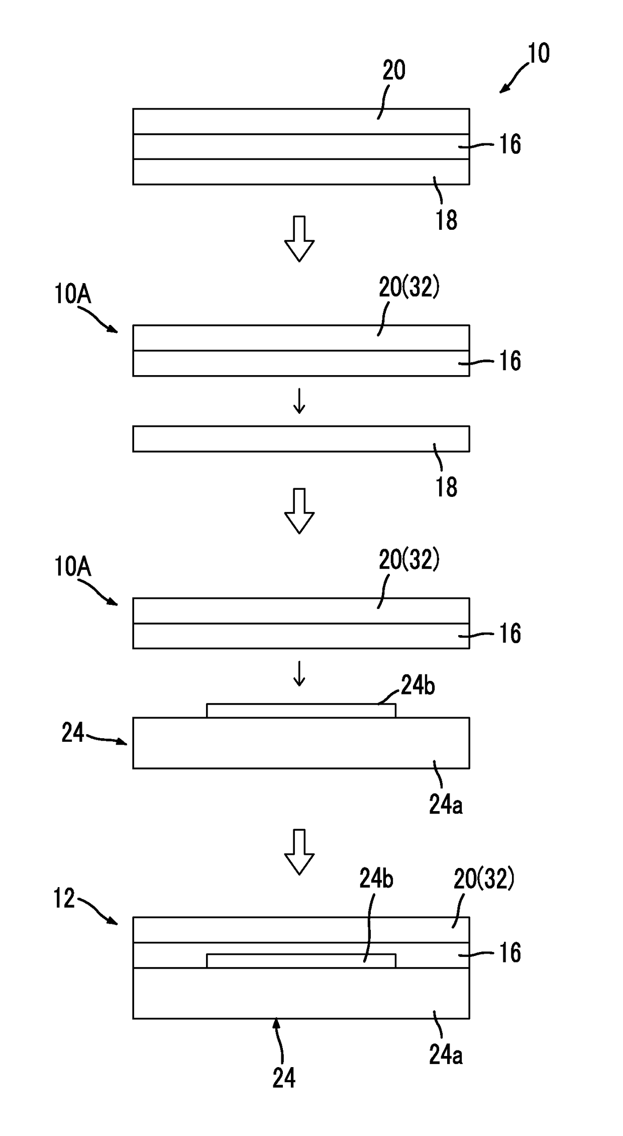
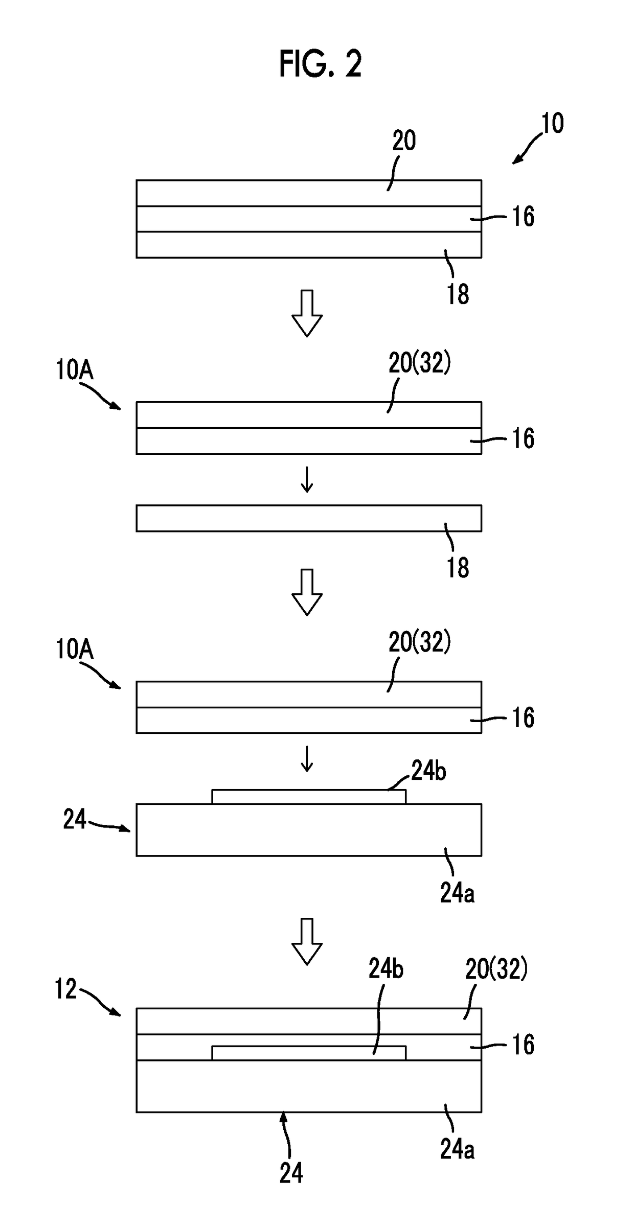
[0145]As the first film 18 and the second film 20, a film obtained by forming a PDMS film having a thickness of 5 μm on the surface of a TAC film having a thickness of 40 μm as a peeling layer was prepared respectively.

[0146]The moisture vapor transmission rate of the first film 18 which was measured in conformity with JIS Z 0208-1976 was 2050 g / (m2·day).

[0147]The peeling layer of the first film 18 was coated with a liquid resin (SK DYNE 1831, manufactured by Soken Chemical & Engineering Co., Ltd.) of two-liquid thermosetting type acrylic ester. The liquid resin was applied using an applicator.

[0148]Next, the peeling layer was directed toward the liquid resin, the second film 20 was laminated, and the liquid resin was cured at 80° C. for 30 minutes, thereby preparing the composite film 10 obtained by bonding the first film 18 and the second film 20 to the pressure sensitive adhesive layer 16 having a thickness of 20 μm.

[0149]The composite film 10 was put into a glove box in which th...

example 2

[0153]The composite film 10 was prepared in the same manner as in Example 1 except that the gas barrier layer 30 was directed toward the pressure sensitive adhesive layer 16 and the gas barrier film 26 was bonded to the pressure sensitive adhesive layer 16 using the gas barrier film 26 prepared in advance as the second film 20.

[0154]The composite film 10 was put into a glove box in which the dew point was adjusted to −60° C. Further, all the subsequent processes were performed in the glove box in which the dew point was adjusted to −60° C.

[0155]The composite film 10 which was put into the glove box was subjected to a heat treatment in the same manner as in Example 1 and then the pressure sensitive adhesive layer 16 was dried.

[0156]The composite film 10 was cooled to room temperature and then the first film 18 was peeled. Next, the composite film 10A from which the first film 18 was peeled was bonded to the organic EL device body 24 prepared in advance, and then the organic EL device...

example 3

[0157]The organic EL device 12 was prepared in the same manner as in Example 1 except that the second film 20 of the composite film 10 was made into a film obtained by forming a film of an ethylene-vinyl acetate (EVA) copolymer having a thickness of 5 μm on the surface of a PET film having a thickness of 50 m as a peeling layer.


PUM

PropertyMeasurementUnit
temperatureaaaaaaaaaa
peel strengthaaaaaaaaaa
thicknessaaaaaaaaaa

Abstract

Provided is a method of manufacturing an electronic device including: drying a pressure sensitive adhesive layer of a composite film which has the pressure sensitive adhesive layer; and a first film and a second film bonded to each surface of the pressure sensitive adhesive layer and in which a moisture vapor transmission rate of the first film at a temperature of 40° C. and a relative humidity of 90% is 100 g / (m2·day) or greater; peeling the first film from the composite film in which the pressure sensitive adhesive layer is dried; and bonding the composite film from which the first film is peeled to an electronic device. In this manner, deterioration of the electronic device due to moisture can be prevented during the manufacture of a laminated electronic device formed by sealing the electronic device with a gas barrier film or the like.

Description

CROSS-REFERENCE TO RELATED APPLICATIONS[0001]This application is a Continuation of PCT International Application No. PCT / JP2015 / 067756 filed on Jun. 19, 2015, which claims priority under 35 U.S.C. §119(a) to Japanese Patent Application No. 2014-132989 filed on Jun. 27, 2014. The above application is hereby expressly incorporated by reference, in its entirety, into the present application.BACKGROUND OF THE INVENTION[0002]1. Field of the Invention[0003]The present invention relates to a method of manufacturing an electronic device such as an organic EL device sealed by a gas barrier film or the like and a composite film used in the method of manufacturing the electronic device.[0004]2. Description of the Related Art[0005]Electronic devices which deteriorate due to moisture, such as organic EL devices or solar cells, are sealed by various sealing members. The electronic devices are typically sealed by glass. Meanwhile, for the purpose of weight reduction or improving impact resistance,...

Claims


Application Information

Patent Timeline
Patent Type & Authority Applications(United States)
IPC IPC(8): B32B38/00B32B7/12H01L51/52B32B37/12H01L51/56B32B7/06B32B23/08B32B7/02
CPCB32B38/164B32B7/06B32B7/12B32B23/08B32B37/12B32B2038/166H01L51/5253B32B2307/7242B32B2457/206B32B2457/12H01L51/56B32B9/02B32B27/00B32B38/10B32B2309/105B32B7/02B32B15/082B32B15/085B32B15/088B32B15/09B32B17/00B32B23/042B32B27/08B32B27/28B32B27/281B32B27/302B32B27/304B32B27/308B32B27/32B32B27/325B32B27/36B32B27/365B32B2250/02B32B2250/24B32B2255/06B32B2255/10B32B2255/20B32B2255/24B32B2255/26B32B2255/28B32B2307/206B32B2307/40B32B2307/412B32B2457/00B32B2457/202H10K50/00H10K50/844B32B43/006H10K71/80H10K50/8426H10K71/00
Inventor KANO, KENJI
Owner FUJIFILM CORP
Why Eureka
Try Eureka