Supercharge Your Innovation With Domain-Expert AI Agents!

Flash memory and fabricating method thereof

a flash memory and fabrication method technology, applied in the field of flash memory, can solve the problems of reducing the size of the flash memory cell, affecting the interaction affecting the performance of adjacent memory cells,

Active Publication Date: 2017-05-04
SEMICON MFG INT (SHANGHAI) CORP +1
View PDF0 Cites 9 Cited by
  • Summary
  • Abstract
  • Description
  • Claims
  • Application Information

AI Technical Summary

Benefits of technology

The patent describes a flash memory and a method of manufacturing it. The method involves depositing a layer of dielectric material to insulate neighboring memory cells. However, the process can create air gaps between the cells, which can cause interference and decrease the performance of the memory. The patent proposes using a high temperature in the deposition process to evaporate water absorbed in a functional layer, which can form air flows that resist the deposition of the dielectric material. This reduces parasitic capacitance and avoids interference between neighboring memory cells.

Problems solved by technology

However, as the size of the flash memory cells reduces, the pitch between adjacent memory cells becomes smaller.
Therefore, the adjacent memory cells may be interfered with each other when reading, writing or erasing operations are performed.
Such interferences may result in an unreliable performance of the flash memory.

Method used


Image

  • Flash memory and fabricating method thereof
  • Flash memory and fabricating method thereof
  • Flash memory and fabricating method thereof

Examples


Embodiment Construction

[0031]Various objects, features, and advantages of the disclosed subject matter can be more fully appreciated with reference to the following detailed description of the disclosed subject matter when considered in connection with the following drawings, in which like reference numerals identify like elements. It should be noted that the following drawings are merely examples for illustrative purposes according to various disclosed embodiments and are not intended to limit the scope of one disclosure.

[0032]It is apparent that the described embodiments are some but not all of the embodiments of the present invention. Based on the disclosed embodiments, persons of ordinary skill in the art may derive other embodiments consistent with the present disclosure, all of which are within the scope of the present invention.

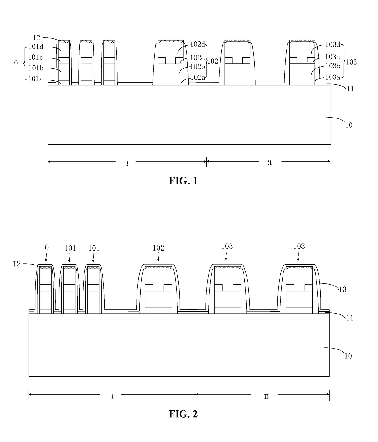
[0033]As described in the background section, with the size reduction of the flash memory cells, the pitch between adjacent memory cells becomes smaller. Therefore, the adja...


PUM


Abstract

In some embodiments, a flash memory and a fabricating method thereof are provided. The method includes proving a substrate including multiple memory transistors and selecting transistors; forming a functional layer covering outer surfaces of the memory transistors and selecting transistors, and surfaces of the substrate between adjacent memory transistors and selecting transistors; performing a surface roughening treatment to the functional layer to provide a roughed surface of the functional layer that absorbs water; and forming a dielectric layer using a chemical vapor deposition (CVD) process, the absorbed water is evaporated from the functional layer during the CVD process to form an upward air flow that resists the deposition of the dielectric layer, such that air gaps are formed between adjacent memory transistors, and the dielectric layer covers top surfaces of the plurality of memory transistors and selecting transistors and fills gaps between each selecting transistor and corresponding adjacent memory transistor.

Description

CROSS-REFERENCES TO RELATED APPLICATIONS[0001]This application claims the priority of Chinese patent application No. 201510714032.2, filed on Oct. 28, 2015, the entire content of which is incorporated herein by reference.TECHNICAL FIELD[0002]The present disclosure generally relates to the field of semiconductor technologies and, more particularly, relates to a flash memory and a method for fabricating the flash memory.BACKGROUND[0003]In the current semiconductor industry, integrated circuit products can be divided into three categories: analog circuits, digital circuits, and digital / analog hybrid circuits. Memory device is one important type of the digital circuits. In recent years, flash memory is particularly rapidly developed in memory device filed. A main feature of the flash memory is that the storage information can be maintained for a long term in an unpowered condition. So flash memories are widely used in rewritable data storages that require a variety of data to be stored ...

Claims


Application Information

Patent Timeline
Patent Type & Authority Applications(United States)
IPC IPC(8): H01L27/115H01L21/02H01L21/764H01L29/06H01L21/28H01L29/51H01L29/49H01L29/788H01L21/322H01L21/311H10N97/00
CPCH01L27/11534H01L21/02337H01L27/11524H01L21/02271H01L21/764H01L21/02359H01L21/31116H01L21/02208H01L29/7883H01L29/0649H01L21/02164H10B41/00H10B99/00H01L21/7682H01L28/00H01L21/02343H01L21/823481H10B41/35H10B41/41H10B41/43H10B41/46
Inventor CHEN, LIANGCHIU, SHENGFEN
Owner SEMICON MFG INT (SHANGHAI) CORP
Features
  • R&D
  • Intellectual Property
  • Life Sciences
  • Materials
  • Tech Scout
  • Unparalleled Data Quality
  • Higher Quality Content
  • 60% Fewer Hallucinations
Learn More