Ultraviolet light-emitting diode

Inactive Publication Date: 2017-05-18
LEXTAR ELECTRONICS CORP
View PDF2 Cites 7 Cited by
  • Summary
  • Abstract
  • Description
  • Claims
  • Application Information

AI Technical Summary

Benefits of technology

[0007]An objective of the present invention is to provide an ultraviolet LED, which uses a

Problems solved by technology

Consequently, the problem of inferior light-emitting efficiency for LEDs may occur.
Nonetheless, the lattice mismatch problem still exists.
The

Method used


Image

  • Ultraviolet light-emitting diode
  • Ultraviolet light-emitting diode
  • Ultraviolet light-emitting diode

Examples


first embodiment

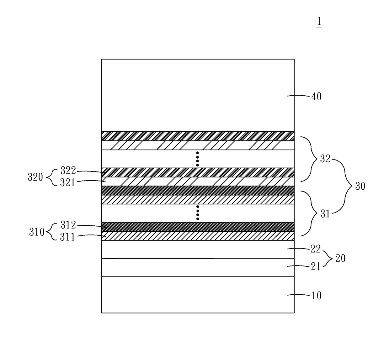
[0027]Please refer to FIGS. 1 and 2, which show schematic diagrams of the ultraviolet LED and improvements according to the present invention. As shown in the figures, the present embodiment provides an epitaxial structure 1 of the ultraviolet LED. The epitaxial structure 1 comprises a substrate 10, a buffer layer 20, a gradual superlattice 30, and an n-type semiconductor layer 40. The gradual superlatticc layer 30 comprises a first superlattice layer 31 and a second superlattice layer 32. According to the present invention, the gradual superlattice layer 30 is used for improving the quality of the epitaxial structure 1 of the ultraviolet LED.

[0028]According to the present embodiment, the material of the substrate 10 may be sapphire, glass, or ceramics. According to the present embodiment, a sapphire substrate is adopted for example. The buffer 20 is disposed on the substrate 10. The buffer layer 20 further comprises a first buffer layer 21 and a second buffer layer 22. The first bu...

second embodiment

[0032]Please refer to FIG. 3, which shows a schematic diagram of the ultraviolet LED according to the present invention. As shown in the figure, the difference between the present embodiment and the first one is that the n-type semiconductor layer 40 according to the present embodiment includes the aluminum gallium nitride (AlGaN) material. According to the order of epitaxy, the ultraviolet LED comprises a first n-type semiconductor layer 41, a second n-type semiconductor layer 42, and a third n-type semiconductor layer 43. The second n-type semiconductor 42 is undoped. The doping concentration of the first n-type semiconductor layer 41 is greater than that of the third n-type semiconductor layer 43. In addition, the first and third n-type semiconductor layers are doped with silicon 33. Moreover, the thickness of the first n-type semiconductor layer 41 is greater than the thickness of the second n-type semiconductor layer 42 and the thickness of the third n-type semiconductor layer ...

third embodiment

[0034]Please refer to FIG. 4, which shows a schematic diagram of the ultraviolet LED according to the present invention. As shown in the figure, according to the present embodiment, the gradual superlattice layer 30 is further doped with silicon with the purpose of facilitating epitaxial growth on the second buffer layer 22 (an undoped aluminum nitride (u-AlN) layer) of the buffer layer 20.

[0035]To sum up, the present invention provides an ultraviolet LED. The gradual superlattice layer is disposed between the buffer layer and the n-type semiconductor layer. The gradual superlattice layer comprises a first superlattice layer and a second superlattice layer. The first superlattice layer includes a multi-layer structure having repetitive stacks of a unit formed by a first layer and a second layer. The second superlattice layer includes a multi-layer structure having repetitive stacks of a unit formed by a third layer and a fourth layer. The concentrations of aluminum in the first, sec...


PUM


Abstract

The present invention relates to an ultraviolet light-emitting diode (LED), which includes a gradual superlattice layer. The gradual superlattice layer comprises a first superlattice layer and a second superlattice layer. The first superlattice layer includes a multi-layer structure having repetitive stacks of a unit formed by a first layer and a second layer. The second superlattice layer includes a multi-layer structure having repetitive stacks of a unit formed by a third layer and a fourth layer. The concentrations of aluminum in the first, second, third, and fourth layers decrease sequentially. By disposing the gradual superlattice layer, the quality of the epitaxial structure may be improved apparently.

Description

FIELD OF THE INVENTION[0001]The present invention relates generally to an ultraviolet light-emitting diode (LED), and particularly to an ultraviolet LED capable of improving the quality of epitaxial structure.BACKGROUND OF THE INVENTION[0002]Technologies advance day by day. The LED industry is developing prosperously. LEDs are widely used in many applications, including lighting, medical, sterilizing, water purifying, and high-density optical recording applications. In particular, ultraviolet LEDs attract additional attention.[0003]Currently, the group-III nitrides are mostly adopted as the semiconductor material for forming LEDs. Thanks to their epitaxial characteristics, the group-II nitrides are applied extensively to electronic equipment or light-emitting devices. Thereby, the epitaxy of the group-III nitrides has become the dominant factor determining the efficiency of electronic equipment or light-emitting devices. While growing a group-III nitride on a substrate, dislocations...

Claims


Application Information

Patent Timeline
IPC IPC(8): H01L33/12H01L33/32H01L33/02H01L33/06
CPCH01L33/12H01L33/025H01L33/32H01L33/06H01L33/04
Inventor YANG, CHUNG-CHIEHWANG, TE-CHUNG
Owner LEXTAR ELECTRONICS CORP
Why Eureka
Try Eureka