Semiconductor device

a technology of semiconductor devices and semiconductors, applied in semiconductor devices, semiconductor/solid-state device details, electrical apparatus, etc., can solve the problems of increasing the ineffective region, affecting the miniaturization of semiconductor devices, and a high probability of hot carriers being trapped in the insulating film, so as to reduce the size and leakage current

Inactive Publication Date: 2017-06-01
MITSUBISHI ELECTRIC CORP
View PDF2 Cites 5 Cited by
  • Summary
  • Abstract
  • Description
  • Claims
  • Application Information

AI Technical Summary

Benefits of technology

[0006]The present invention has been accomplished to solve the above-described problems, and an object of the present invention is to provide a semiconductor device in which a leakage current and a size can be reduced.
[0008]In the present invention, the semi-insulating film directly contacting the semiconductor substrate is used as the passivation film covering the edge termination region. Thus, hot carriers generated in reverse bias are not taken into the semi-insulating film, and the formation of space charge can be inhibited. Accordingly, interface states and the positive charge density between the passivation film and the semiconductor substrate can be kept low. Thus, when the semiconductor device using the planar edge termination region is reversely biased, depletion on the surface of the semiconductor substrate is not hindered, and the electric field can be prevented from extremely increasing. As a result, a leakage current can be reduced, and breakdown voltage stability can be improved. This eliminates the necessity of elongating the edge termination region. Accordingly, the size of the semiconductor device can be reduced.

Problems solved by technology

In particular, in an edge termination region, since the edge termination region is floating, the hot carriers generated are injected into an insulating film which is a conventional passivation film, and part of the hot carriers are likely to be trapped into the insulating film.
Accordingly, an ineffective region increases to inhibit semiconductor device miniaturization.

Method used


Image

  • Semiconductor device
  • Semiconductor device
  • Semiconductor device

Examples


Embodiment Construction

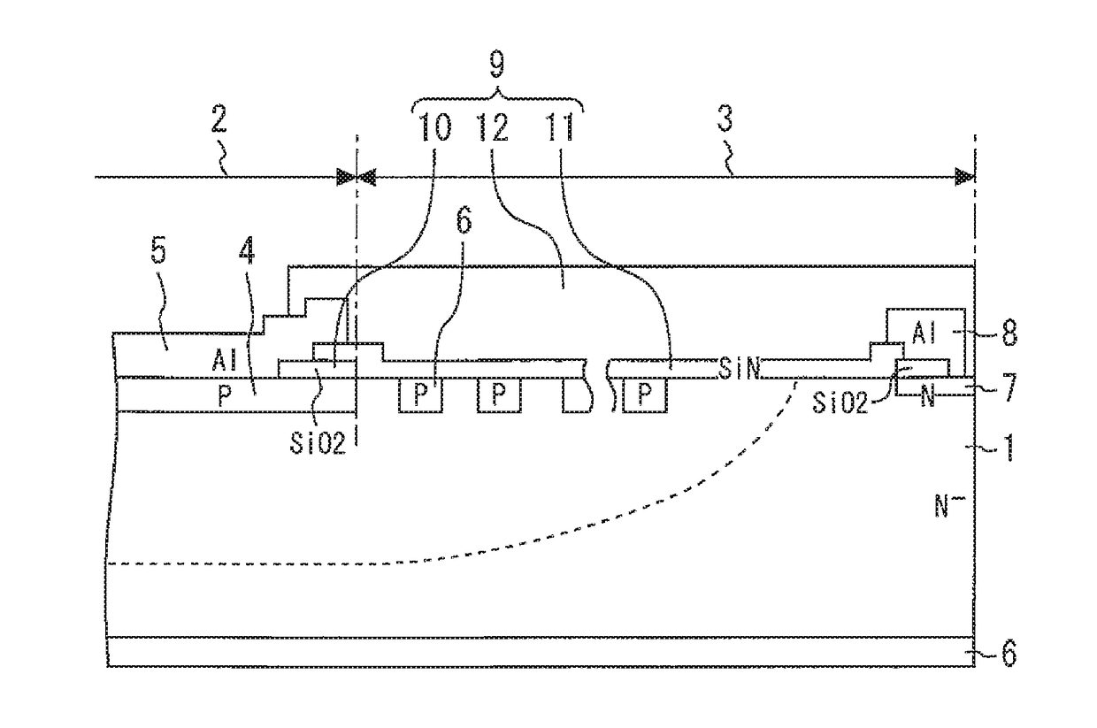
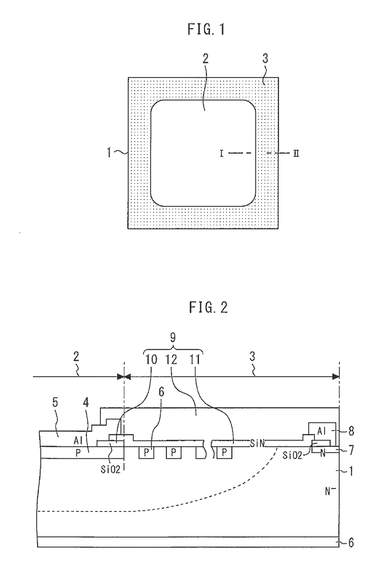
[0013]FIG. 1 is a plan view showing a semiconductor device according to an embodiment of the present invention. A device region 2 is formed in a central portion of a semiconductor substrate 1. A planar edge termination region 3 is formed on the semiconductor substrate 1 to surround the device region 2.

[0014]FIG. 2 is a cross-sectional view taken along line I-II of FIG. 1. In the device region 2, a P-type anode layer 4 is formed on a front side of the N−-type semiconductor substrate 1. An anode electrode 5 made of Al is formed on the P-type anode layer 4. A cathode electrode 6 is formed on a back side of the semiconductor substrate 1. The device region 2 functions as a diode.

[0015]In the edge termination region 3, a plurality of ring-shaped P-type ring layers 6 are formed on the front side of the semiconductor substrate 1 to surround the P-type anode layer 4. A channel stopper 7 made of an N-type diffusion layer is formed to surround the P-type ring layers 6. An Al electrode 8 is con...


PUM


Abstract

A semiconductor device includes: a semiconductor substrate; a device region on the semiconductor substrate; a planar edge termination region on the semiconductor substrate to surround the device region; and a passivation film covering the edge termination region, wherein the passivation film includes a semi-insulating film directly contacting the semiconductor substrate.

Description

BACKGROUND OF THE INVENTION[0001]Field[0002]The present invention relates to a semiconductor device including a planar edge termination region.[0003]Background[0004]In conventional semiconductor devices, an insulating film has been used as a passivation film for covering a planar edge termination region (e.g., see Japanese Patent Application Publication No. 2010-003762).[0005]When a semiconductor device is reversely biased, a high electric field region is formed, and electrons pulled by the high electric field become hot carriers. In particular, in an edge termination region, since the edge termination region is floating, the hot carriers generated are injected into an insulating film which is a conventional passivation film, and part of the hot carriers are likely to be trapped into the insulating film. An increase in space charge in the insulating film tends to increase interface states and the positive charge density at an interface between the insulating film and a semiconductor...

Claims


Application Information

Patent Timeline
Patent Type & Authority Applications(United States)
IPC IPC(8): H01L29/06
CPCH01L29/0615H01L23/3171H01L23/3192H01L29/8611H01L29/0619H01L29/0638H01L29/1602H01L29/1608H01L29/2003
Inventor HARADA, TATSUOHONDA, SHIGETONISHII, AKITOCHEN, ZE
Owner MITSUBISHI ELECTRIC CORP
Why Eureka
Try Eureka