Method of manufacturing semiconductor device and semiconductor device

a manufacturing method and technology of semiconductor devices, applied in the direction of manufacturing tools, metal working devices, welding/soldering/cutting articles, etc., can solve problems such as difficulty in improving productivity, and achieve the effect of simple high mobility and low cos

Inactive Publication Date: 2017-06-01
FUJIFILM CORP
View PDF3 Cites 0 Cited by
  • Summary
  • Abstract
  • Description
  • Claims
  • Application Information

AI Technical Summary

Benefits of technology

[0031]For this reason, according to the invention, it is possible to manufacture a semiconductor dev

Problems solved by technology

However, it is very challenging to form an organic semiconductor film at proper positions correspo

Method used


Image

  • Method of manufacturing semiconductor device and semiconductor device
  • Method of manufacturing semiconductor device and semiconductor device
  • Method of manufacturing semiconductor device and semiconductor device

Examples


Embodiment Construction

[0038]Hereinafter, a method of manufacturing a semiconductor device and a semiconductor device of the invention will be described in detail based on a suitable example shown in the accompanying drawings.

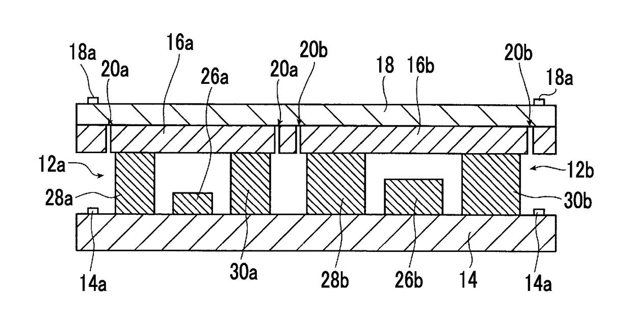
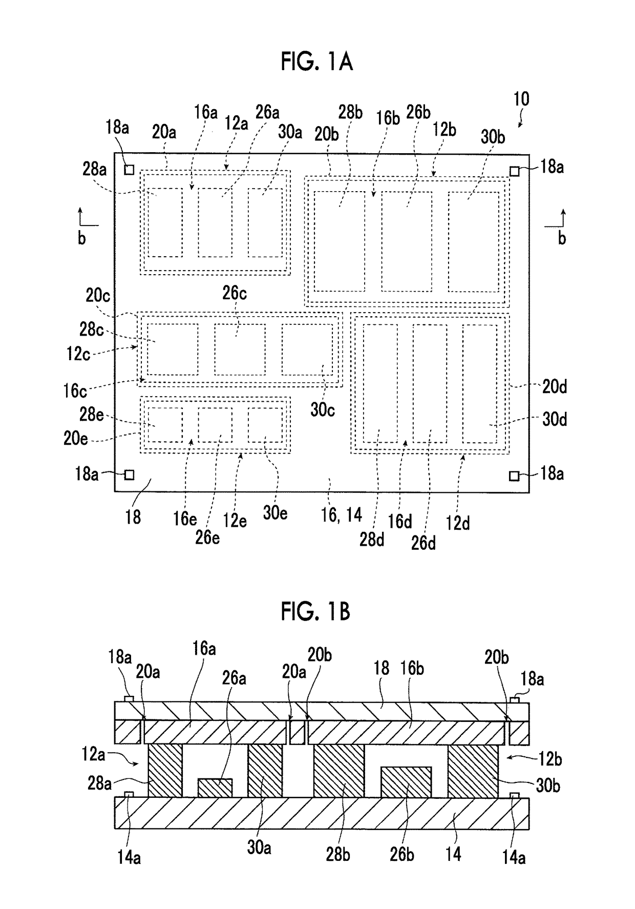
[0039]FIGS. 1A and 1B conceptually show an example of a semiconductor device of the invention manufactured by the method of manufacturing a semiconductor device of the invention. FIG. 1A is a top view, and FIG. 1B is a cross-sectional view taken along the line b-b of FIG. 1A.

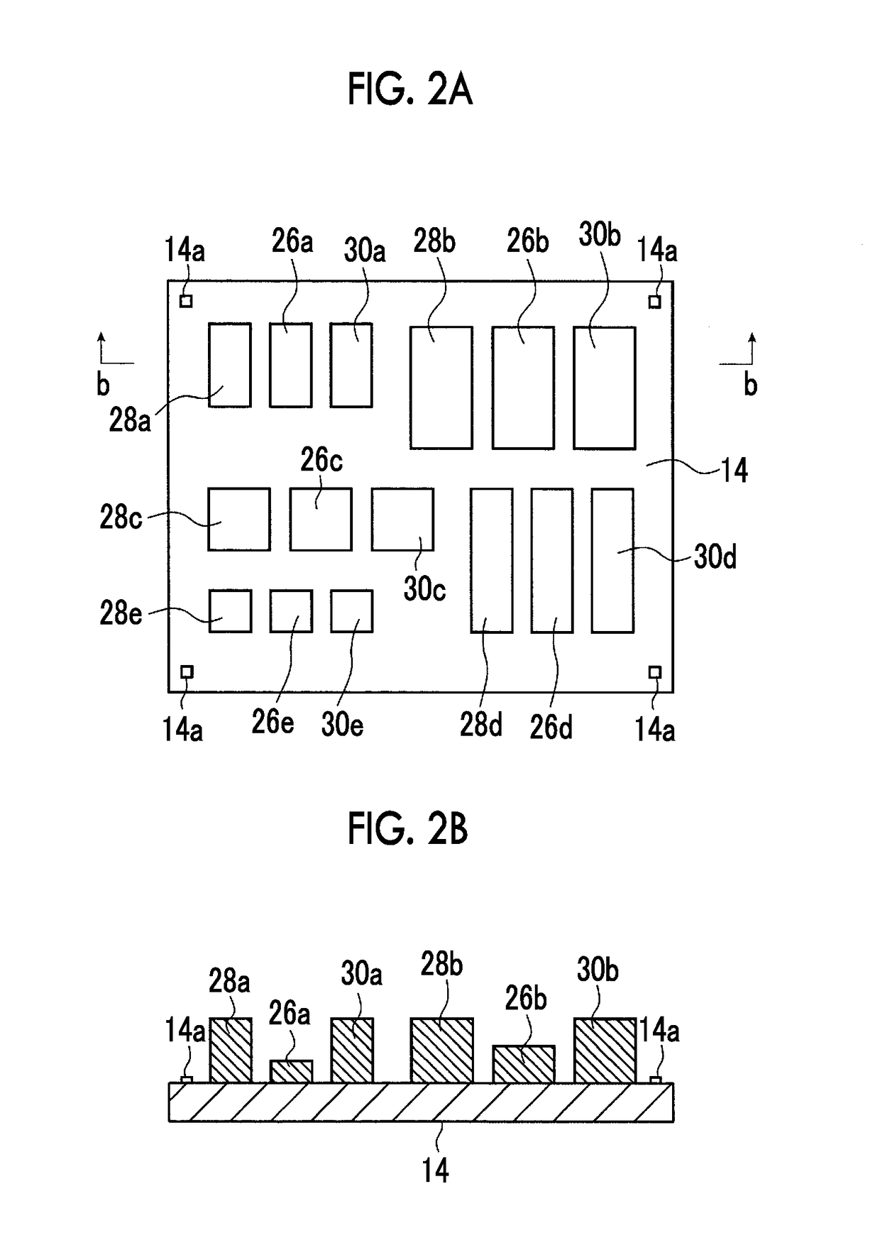
[0040]A semiconductor device 10 of the illustrated example is a semiconductor device having five organic semiconductor elements 12a to 12e. Specifically, the semiconductor device 10 has an insulating substrate 14, the organic semiconductor elements 12a, 12b, 12c, 12d, and 12e, an organic semiconductor film 16, and an insulating support 18.

[0041]In the organic semiconductor film 16, divided regions 16a to 16e divided corresponding to the respective organic semiconductor elements by grooves 20a to 20e are formed. T...


PUM


Abstract

Disclosed are a manufacturing method capable of manufacturing a semiconductor device having a plurality of organic semiconductor elements with a simple process and high productivity, and a semiconductor device. This problem is solved by forming, on an insulating substrate, electrodes corresponding to a plurality of semiconductor elements, in which the position of an uppermost portion of each of a source electrode and a drain electrode is higher than that of a gate electrode, forming an organic semiconductor film on a surface of an insulating support, forming grooves in the organic semiconductor film to form divided regions according to the individual semiconductor elements, and aligning and laminating the insulating support and the insulating substrate.

Description

CROSS-REFERENCE TO RELATED APPLICATIONS[0001]This application is a Continuation of PCT International Application No. PCT / JP2015 / 073156 filed on Aug. 18, 2015, which claims priority under 35 U.S.C. §119(a) to Japanese Patent Application No. 2014-190135 filed on Sep. 18, 2014. The above application is hereby expressly incorporated by reference, in its entirety, into the present application.BACKGROUND OF THE INVENTION[0002]1. Field of the Invention[0003]The present invention relates to a method of manufacturing a semiconductor device having a plurality of bottom gate-bottom contact organic semiconductor elements, and a semiconductor device manufactured by the manufacturing method.[0004]2. Description of the Related Art[0005]Various structures of an organic semiconductor element are known according to the positional relationship between a gate electrode, a source electrode, and a drain electrode and an organic semiconductor film. Representatively, four structures of a bottom gate-bottom...

Claims


Application Information

Patent Timeline
IPC IPC(8): H01L51/05B23K26/351
CPCB23K26/351H01L51/0512B23K26/0006B23K26/402B23K26/359B23K26/364B23K26/082B23K26/066B23K2101/42B23K2103/50H10K71/20H10K71/50H10K10/484H10K10/462
Inventor USAMI, YOSHIHISATAKAHASHI, KOUKIMAEHARA, YOSHIKINAKAMURA, SEIGO
Owner FUJIFILM CORP
Why Eureka
Try Eureka