Organic light emitting display device

a light-emitting display and organic technology, applied in the direction of organic semiconductor devices, solid-state devices, semiconductor devices, etc., can solve the problems of degrading the reliability of organic light-emitting devices, and the inability to reduce the manufacturing cost of organic light-emitting display devices, so as to improve efficiency or lifetime, reduce driving voltage, and enhance efficiency or lifetime

Active Publication Date: 2017-06-01
LG DISPLAY CO LTD
View PDF8 Cites 7 Cited by
  • Summary
  • Abstract
  • Description
  • Claims
  • Application Information

AI Technical Summary

Benefits of technology

[0011]Therefore, the inventors recognize the above-described limitations and have done various experiments for enhancing efficiency or lifetime by adjusting characteristic of a hole transport layer adjacent to the P-type charge generation layer which is configured in a structure including no dopant. Through the various experiments, the inventors have invented an organic light emitting display device having a new structure for enhancing efficiency or lifetime.
[0012]An aspect of the present disclosure is directed to provide an organic light emitting display device in which a hole transport layer adjacent to a P-type charge generation layer is configured by a combination of a material, having an absolute value of a lowest unoccupied molecular orbitals (LUMO) energy level which is greater than an absolute value of a LUMO energy level of the P-type charge generation layer, and a material having hole mobility higher than that of the P-type charge generation layer, thereby reducing a driving voltage and enhancing efficiency or lifetime.
[0013]Another aspect of the present disclosure is directed to provide an organic light emitting display device in which a hole transport layer adjacent to a P-type charge generation layer is configured by two layers (for example, a layer having high hole mobility and a layer having electron-blocking characteristic), thereby reducing a driving voltage and enhancing efficiency or lifetime.

Problems solved by technology

In this case, a process of performing co-deposition by adjusting a concentration of the host and the dopant included in the P-type charge generation layer is needed, but the process causes a time-based deviation between organic layers including the organic light emitting device to degrade reliability of the organic light emitting device.
Also, since a P-type dopant material doped on the P-type charge generation layer is expensive, the manufacturing cost of an organic light emitting display device cannot be reduced.

Method used


Image

  • Organic light emitting display device
  • Organic light emitting display device
  • Organic light emitting display device

Examples


first embodiment

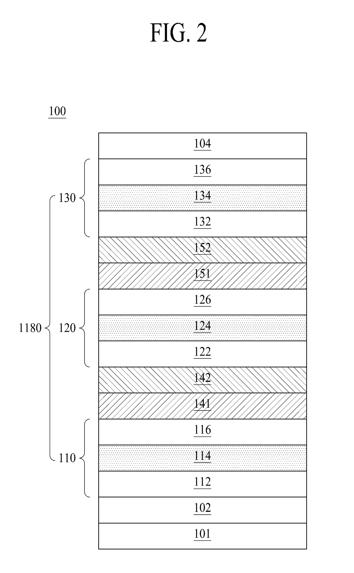
[0051]FIG. 2 is a diagram illustrating an organic light emitting device 100 according to the present disclosure.

[0052]The organic light emitting device 100 illustrated in FIG. 2 may include a substrate 101, a first electrode 102, a second electrode 104, and an emission part 1180 between the first and second electrodes 102 and 104. The emission part 1180 may include a first emission part 110, a second emission part 120, and a third emission part 130.

[0053]The substrate 101 may be formed of an insulating material or a material having flexibility. The substrate 101 may be formed of glass, metal, plastic, and / or the like, but is not limited thereto. If an organic light emitting display device is a flexible organic light emitting display device, the substrate 101 may be formed of a flexible material such as plastic and / or the like. Also, if an organic light emitting device which is easy to realize flexibility is applied to a lighting device for vehicles, various designs and a degree of f...

second embodiment

[0115]FIG. 3 is a diagram illustrating an organic light emitting device 200 according to the present disclosure.

[0116]The organic light emitting device 200 illustrated in FIG. 3 may include a substrate 201, a first electrode 202, a second electrode 204, and an emission part 1180 between the first electrode 202 and the second electrode 204. The emission part 1180 may include a first emission part 210, a second emission part 220, and a third emission part 230. The substrate 201, the first electrode 202, the second electrode 204, and the first emission part 210 illustrated in FIG. 3 may be substantially the same as the substrate 101, the first electrode 102, the second electrode 104, and the first emission part 110 described above with reference to FIG. 1, and thus, their detailed descriptions are not provided herein or will be brief.

[0117]The first emission part 210 may include a first HTL 212, a first EML 214, and a first ETL 216 which are disposed on the first electrode 202.

[0118]Th...

third embodiment

[0166]FIG. 4 is a diagram illustrating an organic light emitting device 300 according to the present disclosure.

[0167]The organic light emitting device 300 illustrated in FIG. 4 may include a substrate 301, a first electrode 302, a second electrode 304, and an emission part 1180 between the first electrode 302 and the second electrode 304. The emission part 1180 may include a first emission part 310, a second emission part 320, and a third emission part 330. The substrate 301, the first electrode 302, the second electrode 304, and the first emission part 310 illustrated in FIG. 4 may be substantially the same as the substrate 101, the first electrode 102, the second electrode 104, and the first emission part 110 described above with reference to FIG. 1, an d thus, their detailed descriptions are not provided herein or will be brief.

[0168]The first emission part 310 may include a first HTL 312, a first EML 314, and a first ETL 316 which are disposed on the first electrode 302.

[0169]A...


PUM


Abstract

Discussed is an organic light emitting display device. The organic light emitting display device can include a first emission part, a second emission part on the first emission part, and a first P-type charge generation layer between the first emission part and the second emission part. The first emission part includes a first hole transport layer, a first emission layer, and a first electron transport layer. The second emission part includes a second hole transport layer, a second emission layer, and a second electron transport layer. The second hole transport layer and the first P-type charge generation layer are disposed adjacent to each other. The second hole transport layer includes a first material and a second material. The first material has an absolute value of a HOMO energy level which can be greater than an absolute value of a LUMO energy level of the first P-type charge generation layer.

Description

CROSS-REFERENCE TO RELATED APPLICATIONS[0001]This application claims the priority benefit of the Korean Patent Application No. 10-2015-0168749 filed on Nov. 30, 2015, which is hereby incorporated by reference as if fully set forth herein.BACKGROUND OF THE INVENTION[0002]Technical Field[0003]The present disclosure relates to an organic light emitting display device, and more particularly, to an organic light emitting display device in which a driving voltage is reduced and efficiency or lifetime is enhanced.[0004]Discussion of the Related Art[0005]Recently, as society advances to the information-oriented society, the field of display devices which visually express an electrical information signal is rapidly advancing. Various display devices, having excellent performance in terms of thinness, lightness, and low power consumption, are being developed correspondingly.[0006]Examples of the display devices include liquid crystal display (LCD) devices, plasma display panel (PDP) devices, ...

Claims


Application Information

Patent Timeline
Patent Type & Authority Applications(United States)
IPC IPC(8): H01L51/50H01L27/32
CPCH01L51/5004H01L51/504H01L51/5056H01L51/5072H01L51/5088H01L2251/558H01L27/322H01L27/3246H01L27/3248H01L2251/552H01L51/5016H10K59/32H10K50/11H10K2101/40H10K50/131H10K50/155H10K50/15H10K50/19H10K2102/351H10K50/13H10K50/16H10K50/17H10K59/38H10K59/122H10K59/123H10K2101/10H10K2101/30
Inventor HAN, YOONDEOKLEE, JAEMANAHN, SOYEONCHOI, HEEDONGPARK, JUNGSOO
Owner LG DISPLAY CO LTD
Why Eureka
Try Eureka