Grating element
- Summary
- Abstract
- Description
- Claims
- Application Information
AI Technical Summary
Benefits of technology
Problems solved by technology
Method used
Image
Examples
example 1
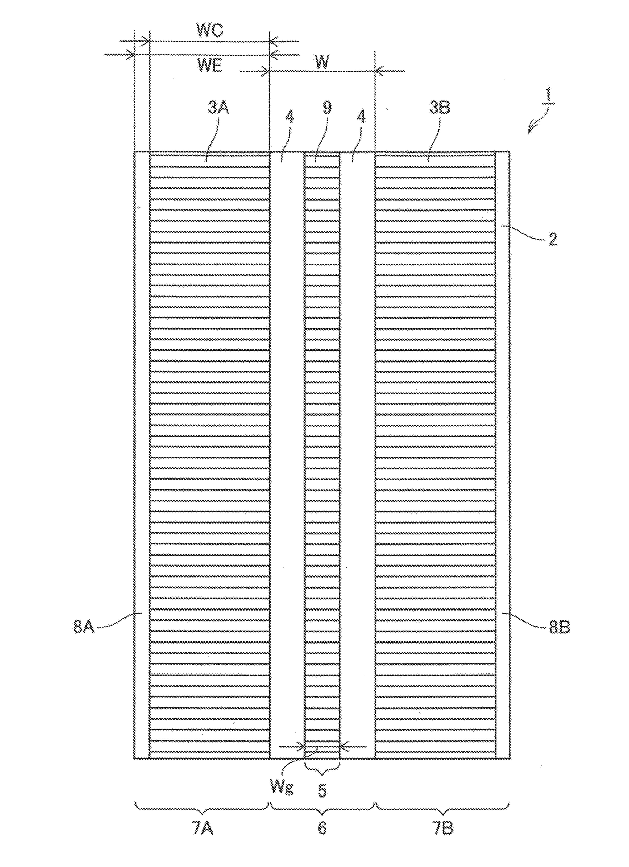
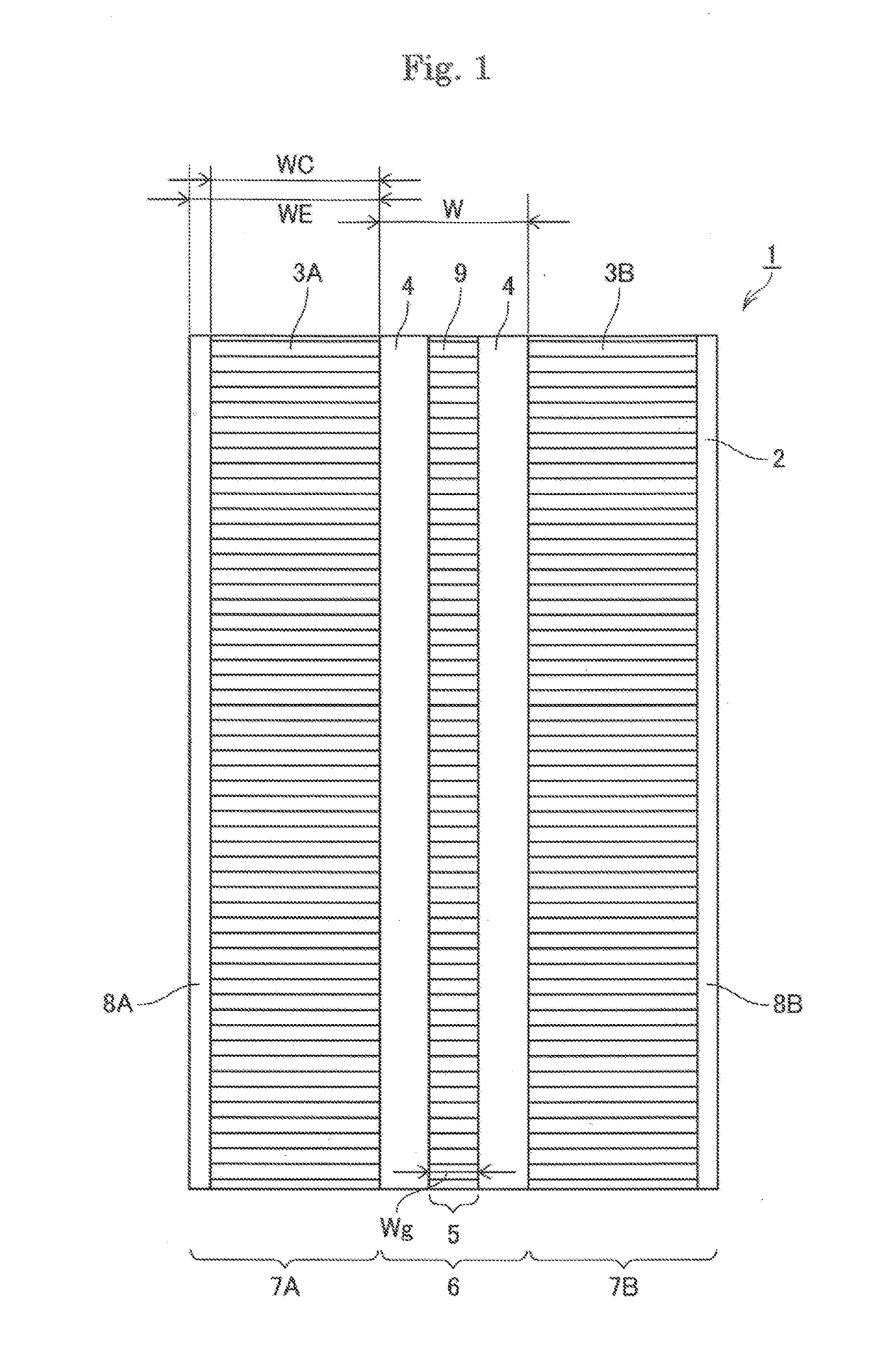
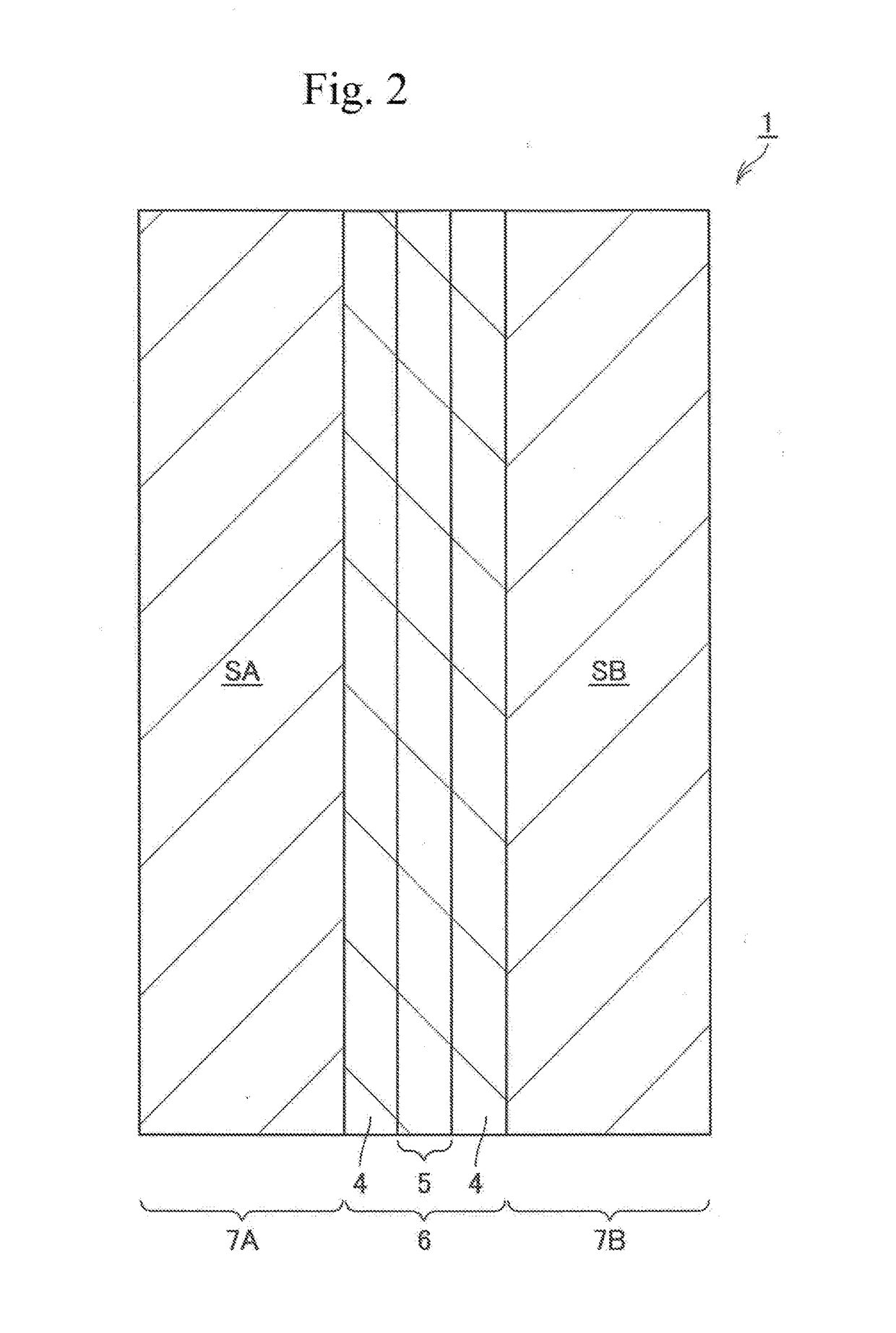
[0086]It was produced a light emitting system as shown in FIGS. 1, 3, 5 and 8.
[0087]Specifically, on a supporting body 11 composed of a silicon wafer, by means of a sputtering apparatus, a lower clad layer 10 made of SiO2 was deposited in a thickness of 1 μm. An optical material layer 20 made of Ta2O5 in a thickness of 1.2 μm was deposited further. Then, Ti was deposited on the optical material layer to produce a grating pattern by nanoimprinting process. As to the grating pattern, the pitch interval Λ was made 206 nm and the length Lb was made 100 μm.
[0088]Thereafter, the Ti film was etched to form a grating pattern of Ti, using a resist pattern, obtained by the nanoimprinting, as a base. Then, the pattern of the Ti film was used as a mask to perform reactive ion etching of fluorine-base to form a Bragg grating having a pitch interval Λ of 206 nm and a length Lb of 100 μm. The depth of the groove of the grating was made 40 nm.
[0089]Further, for forming an optical waveguide, the Ti ...
example 2
[0106]A grating device was produced and evaluated according to the same procedure as that in the Example 1.
[0107]However, different from the Example 1, (area of the Bragg grating 3A +area of the Bragg grating 3B) / (SA+SB) was made 50 percent.
[0108]As to the optical characteristics of the grating device, a reflection center wavelength was 846 nm, the reflectance was 20 percent and the full width at half maximum was 2 nm.
[0109]Driving was conducted under an automatic current control (ACC) without using a Peltier element after the module has been mounted. The laser module had the laser characteristics that oscillation took place at a central wavelength of 846 nm, and an output thereof was 17.5 mW. Further, the optical spot observed at the emitting side end face of the waveguide was substantially of Gaussian distribution, and it was not observed the light of slab mode irradiated from the substrate.
example 3
[0110]A grating device was produced and evaluated according to the same procedure as that in the Example 1.
[0111]However, different from the Example 1, (area of the Bragg grating 3A+area of the Bragg grating 3B) / (SA+SB) was made 100 percent.
[0112]As to the optical characteristics of the grating device, a reflection center wavelength was 846 nm, the reflectance was 20 percent and the full width at half maximum was 2 nm.
[0113]Driving was conducted under an automatic current control (ACC) without using a Peltier element after the module has been mounted. The laser module had the laser characteristics that oscillation took place at a central wavelength of 846 nm, and an output thereof was 18 mW. Further, the optical spot observed at the emitting side end face of the waveguide was substantially of Gaussian distribution, and it was not observed the light of slab mode irradiated from the substrate.
PUM
 Abstract
Description
Claims
Application Information


