Process for preparing quantum dot array and quantum dot superlattice

Active Publication Date: 2017-06-08
TOYOTA JIDOSHA KK
View PDF3 Cites 0 Cited by
  • Summary
  • Abstract
  • Description
  • Claims
  • Application Information

AI Technical Summary

Benefits of technology

[0007]It is an aim of the present invention to provide a new way of preparing quantum dot arrays, which may in preferred embodiments be stacked quantum dot superlattices, and can be used in optoelectronic devices such as solar cells. It is desired to overcome the disadvantages of molecular beam epitaxy (MBE) and related methods which are very demanding in terms of cost, as well as being limited in terms of possible types and minimum purities of precursor materials. The present invention provides a wet room temperature growth process for QDs on a crystalline substrate by a SILAR (successive ionic layer deposition and reaction) metho

Problems solved by technology

On the other hand, their processing is characterized by high costs.
Furthermore, only a few combinations of barrier material/QD pairs are able to be grown due to lattice matching constrain

Method used


Image

  • Process for preparing quantum dot array and quantum dot superlattice
  • Process for preparing quantum dot array and quantum dot superlattice
  • Process for preparing quantum dot array and quantum dot superlattice

Examples


Example

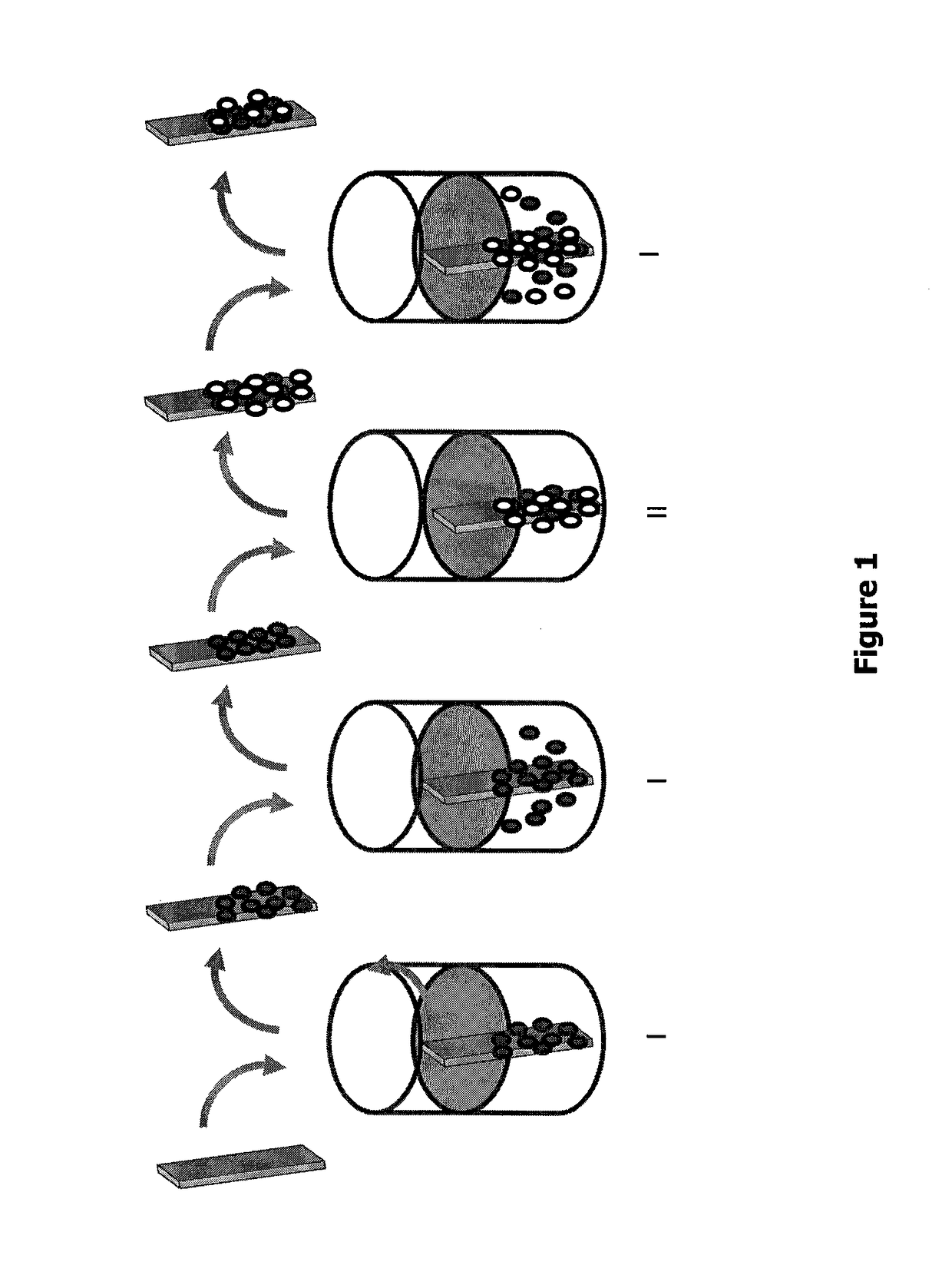
[0017]The Successive Ionic Layer Adsorption and Reaction (SILAR) method is based on triggering successive reactions in solutions such as aqueous (or ethanolic or any other suitable solutions of) saturated ionic solutions with a solid interface, as is illustrated by the dipping of a planar substrate in FIG. 1. Cation and anion dissolved precursors in the solutions will react with the substrate to yield the desired product. FIG. 1 is a schematic diagram showing the growth of an AB compound by a SILAR method. One SILAR cycle refers to (a) A+ ion solution dipping; (b) rinsing-removal of A+ ions in excess; (c) B− ion solution dipping; (d) rinsing-removal of B− ions in excess.

[0018]The nucleation of a QD layer by SILAR follows a protocol analogous to that used for the growth of a thin film (differing only in the amount of material deposited). Control of deposition on the substrate surface to achieve only very small particles (quantum dots) can be achieved by controlling deposition rate (a...


PUM


Abstract

The present invention presents a process for preparing a quantum dot array comprising at least the steps of: (a) providing a crystalline semiconductor substrate surface; (b) depositing quantum dots on the said substrate surface by a process of successive ionic layer adsorption and reaction (SILAR). The steps can be repeated to build up a quantum dot superlattice structure.

Description

FIELD OF THE INVENTION[0001]The present invention seeks to provide a new way of preparing quantum dot arrays, which may in preferred embodiments be stacked quantum dot superlattices, and can be used in optoelectronic devices such as solar cells.TECHNOLOGICAL BACKGROUND TO THE INVENTION[0002]By the term “quantum dots”, reference is made here to nanometer sized particles of semiconductor material where quantum confinement is present. Depending upon the semiconductor material, the maximum sizes change but are usually below 100 nm. The exact size of the quantum dots may enable the semiconductor band gap to be modulated, which provides potential for increasing photo-electric conversion efficiency with respect to bulk films of semiconductor material in more conventional solar cells and related devices.[0003]A three-dimensional ordered matrix of quantum dots (QDs), known as a QD solid (QDS) or a QD superlattice (QD-SL) has a potential in optoelectronic applications, including devices such ...

Claims


Application Information

Patent Timeline
IPC IPC(8): H01L31/0352H01L31/18
CPCH01L31/035218H01L31/035236H01L31/1868H01L31/1836H01L21/0237H01L21/02521H01L21/0256H01L21/02568H01L21/02601H01L21/02628
Inventor KINGE, SACHINCANOVAS DIAZ, ENRIQUEBONN, MISCHA
Owner TOYOTA JIDOSHA KK
Why Eureka
Try Eureka