Selectively doped trench device isolation

Inactive Publication Date: 2005-01-20
MICRON TECH INC
View PDF29 Cites 3 Cited by
  • Summary
  • Abstract
  • Description
  • Claims
  • Application Information

AI Technical Summary

Benefits of technology

[0018] In one embodiment of the present invention, a trench is formed in a field region of a p-type substrate and a thin layer of field oxide is formed on the trench side walls and the floor. The oxide covered trench is then filled with a material having work function value that is higher than the work function value of the p-type substrate. In this embodiment the material is a heavily doped P+ polysilicon material. The higher work function of the P+ polysilicon material produces a high flat band voltage that produces high threshold voltages. This high thresh

Problems solved by technology

This situation presents a special challenge for the isolation structures as these devices must be smaller and yet still provide the necessary isolation.
In fact, the integrity and the reliability of each active device greatly depends on ability to electrically isolate each active device from adjacent active devices as leakage currents from adjacent devices can result in failure.
Although the high field threshold provided by such thick field oxide effectively isolates the active devices, the LOCOS process presents some disadvantages associated with the nature of the oxidation process.
For example, thick isolation structures formed through oxidation consume a considerable amount of area on the chip limiting the amount of area available for active devices and thereby limiting the active device density.
Moreover, during the oxidation process there is lateral encroachment into the active areas of the chip.
This lateral encroachment is known as bird's beak encroachment and it further limits the size of the active areas of the chip and the active device density.
This bird's beak encroachment remains a significant problem even as device dimensions and isolation structure di

Method used


Image

  • Selectively doped trench device isolation
  • Selectively doped trench device isolation
  • Selectively doped trench device isolation

Examples


Embodiment Construction

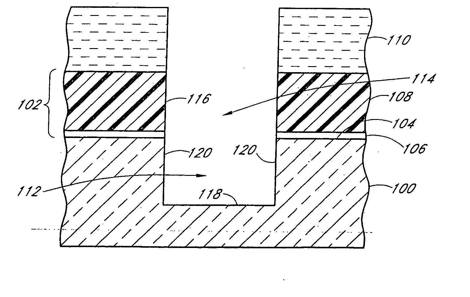
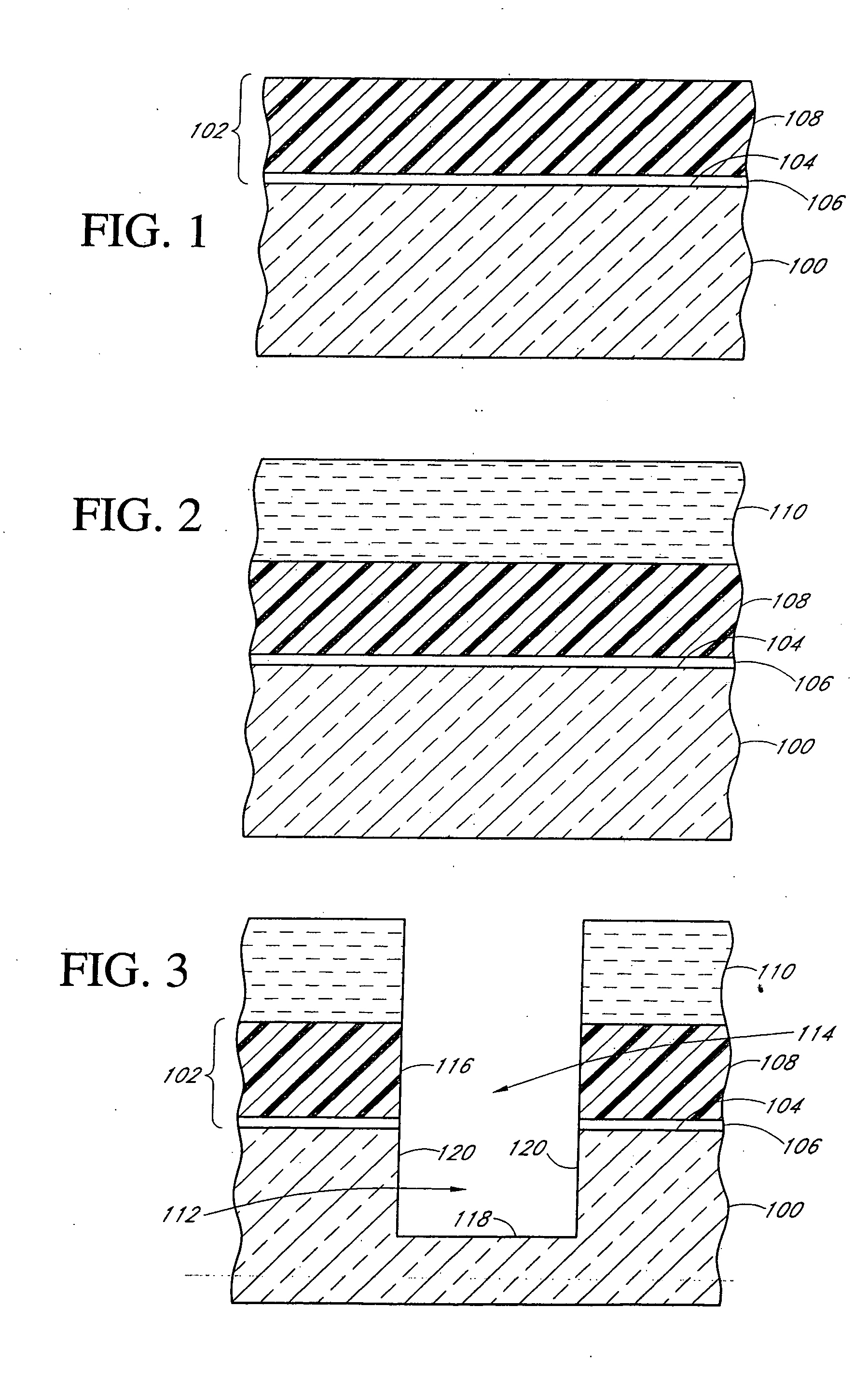
[0029] Reference will now be made to the drawings wherein like numerals refer to like parts throughout. FIG. 1 illustrates a semiconductor substrate 100 where a mask structure 102 is formed on a top surface 104 of the substrate 100. In this embodiment, the semiconductor substrate 100 preferably comprises a p-type silicon substrate, and the mask structure 102 may be comprised of a silicon oxide layer 106 and a nitride layer 108. The silicon oxide layer 106, often referred to as pad-oxide layer, may be formed by oxidation of the top surface 104 using any of a number of well-known wet or dry oxidation techniques so as to grow a silicon oxide layer with a thickness on the order of approximately 30 to 300 Angstroms. The nitride layer 108 may be formed on the pad-oxide layer 106 using any of a well-known deposition processes, preferably a Chemical Vapor Deposition (CVD) process. The nitride layer may preferably be deposited to a thickness of approximately 1000-2500 A.

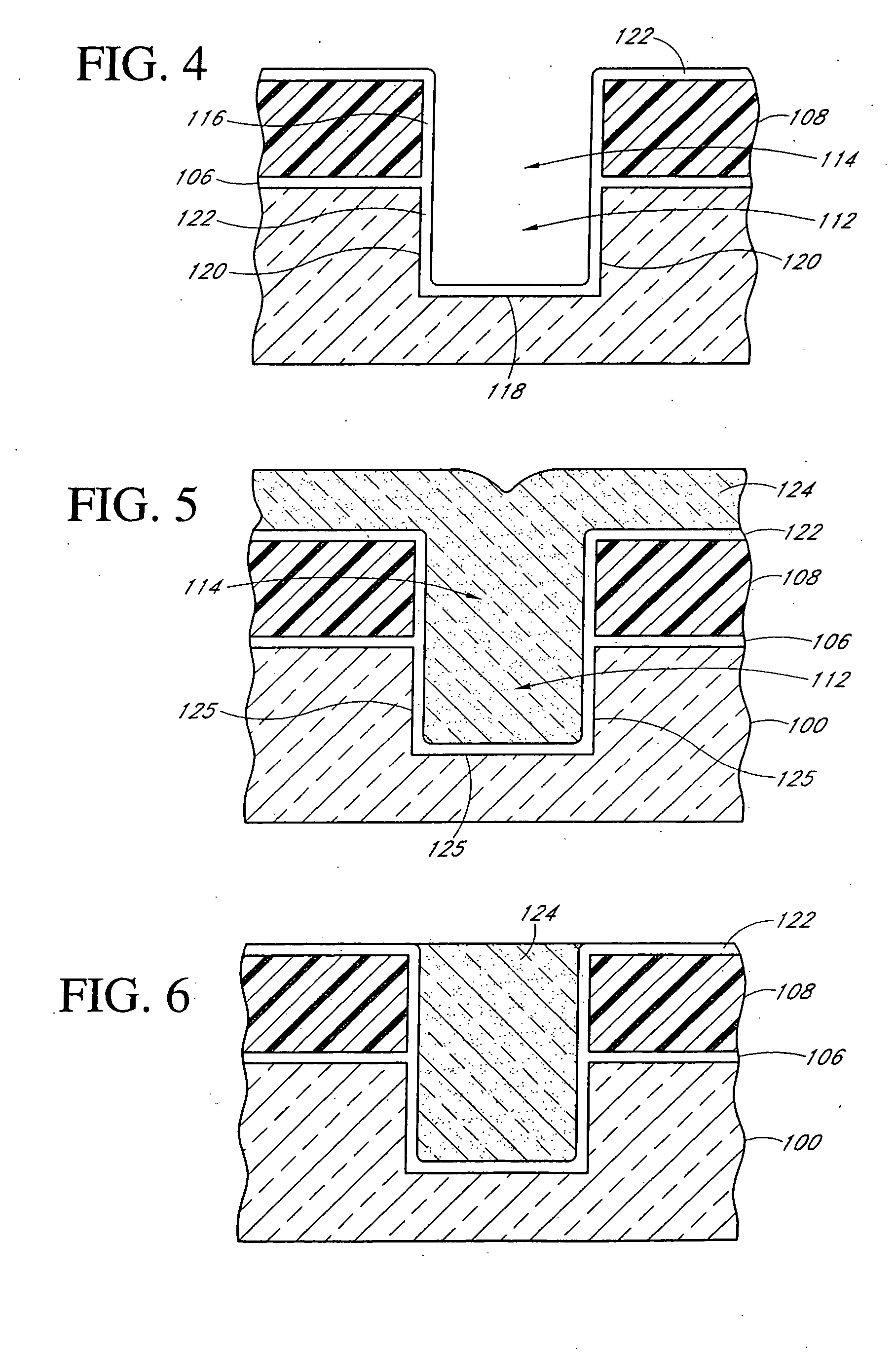
[0030] As shown in F...


PUM


Abstract

A selectively doped trench isolation device is provided. The trench isolation device of the preferred embodiment includes a semiconductor substrate having a trench. A thin field oxide layer is grown on the side walls of the trench, and the trench is filled with a heavily doped polysilicon. The work function difference between the substrate and the heavily doped polysilicon increases the field threshold voltage of the gated trench isolation device so that smaller isolation structures can be formed between adjacent active devices in higher density integrated circuits.

Description

RELATED APPLICATIONS [0001] This Application is a divisional application of U.S. patent application Ser. No. 09 / 143,585 filed Aug. 31, 1998 entitled “SELECTIVELY DOPED TRENCH DEVICE ISOLATION”, which is hereby incorporated by reference in its entirety.BACKGROUND OF THE INVENTION [0002] 1. Field of the Invention [0003] The present invention relates to semiconductor device design and fabrication and more particularly to trench isolation of such devices. [0004] 2. Description of the Related Art [0005] In the semiconductor industry, there is a continuing trend towards increasing the number of components formed in an area of an integrated circuit. This trend is resulting in Ultra Large Scale Integration (ULSI devices). This trend is driving the semiconductor industry to explore new materials and processes for fabricating integrated devices having sub-micron sized features so that more devices can be formed in the same area of an integrated circuit. This is particularly true for the manuf...

Claims


Application Information

Patent Timeline
IPC IPC(8): H01L21/763H01L21/765
CPCH01L21/763H01L21/823481H01L21/765
Inventor KAO, DAVID Y.YANG, RONGSHENG
Owner MICRON TECH INC
Why Eureka
Try Eureka