Nonvolatile semiconductor memory element and nonvolatile semiconductor memory device

Inactive Publication Date: 2008-03-27
KK TOSHIBA
View PDF9 Cites 5 Cited by
  • Summary
  • Abstract
  • Description
  • Claims
  • Application Information

AI Technical Summary

Benefits of technology

[0008]The present invention has been made in view of these circumstances, and an object thereof is to provide high-performance nonvolatile semiconductor memory elements and high-performance nonvolatile semiconductor memory devices that have high controllability over threshold voltages, so as to have more than two different threshold voltages while lowering the power supply voltage.

Problems solved by technology

This fact has greatly hindered the achievement of a low power supply voltage required to reduce power consumption.

Method used


Image

  • Nonvolatile semiconductor memory element and nonvolatile semiconductor memory device
  • Nonvolatile semiconductor memory element and nonvolatile semiconductor memory device
  • Nonvolatile semiconductor memory element and nonvolatile semiconductor memory device

Examples


first embodiment

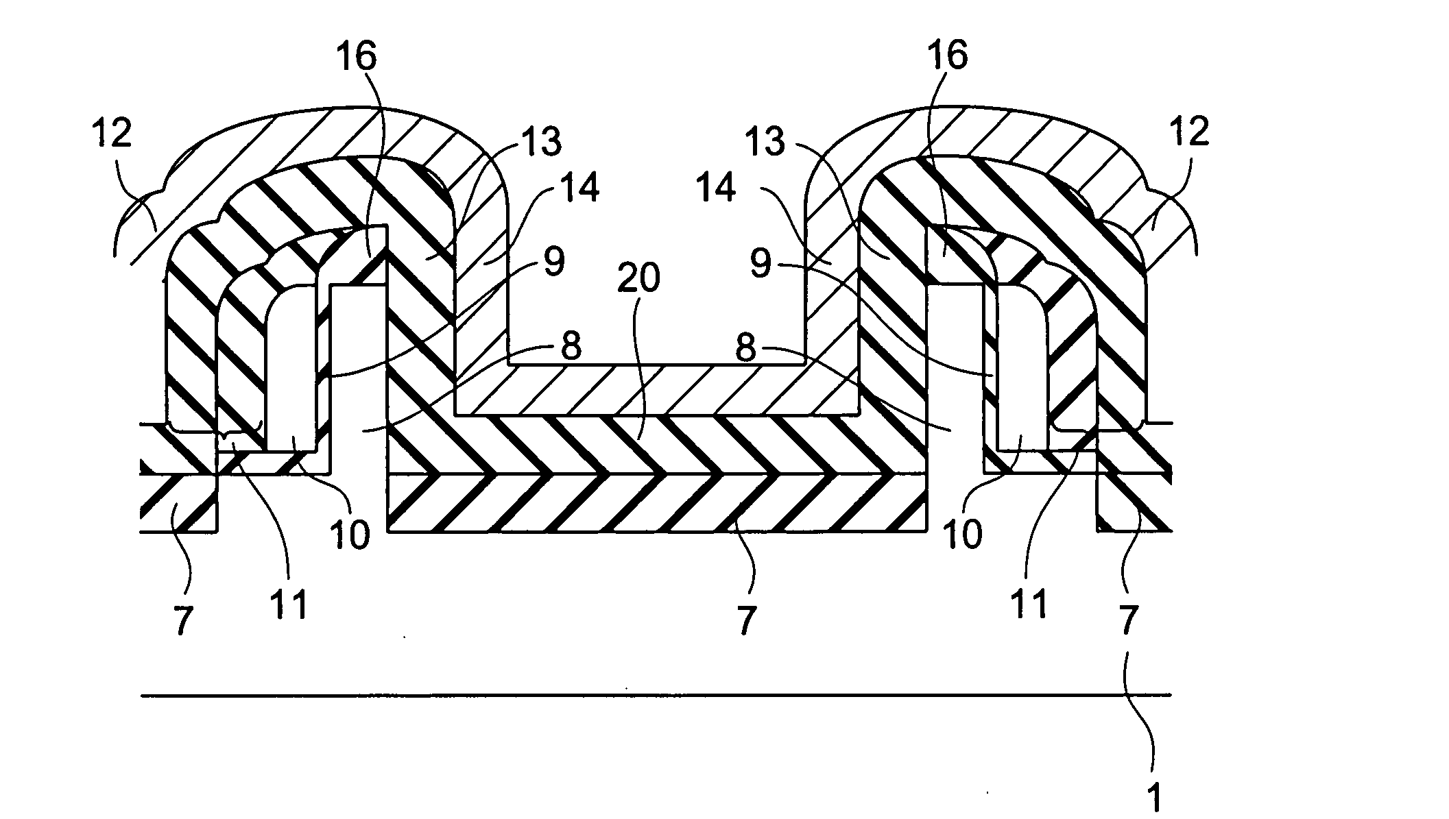
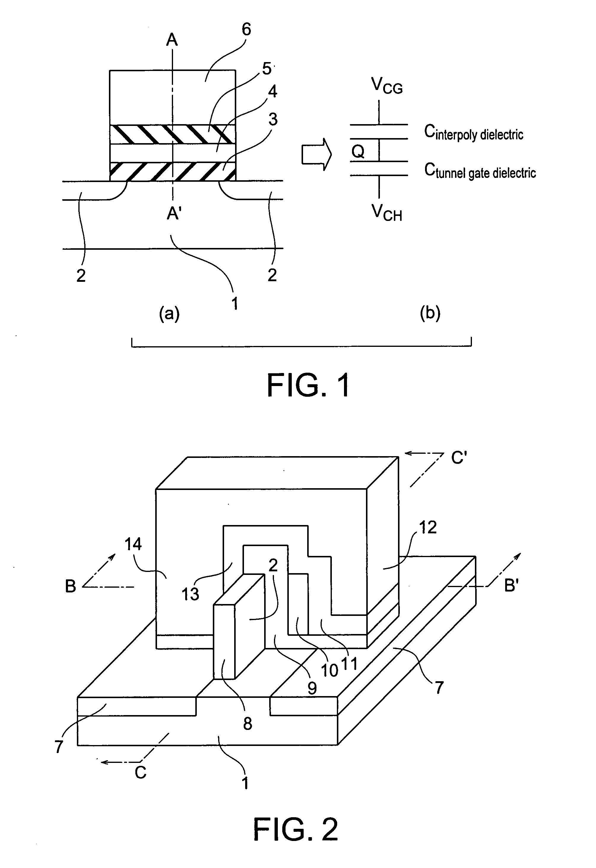
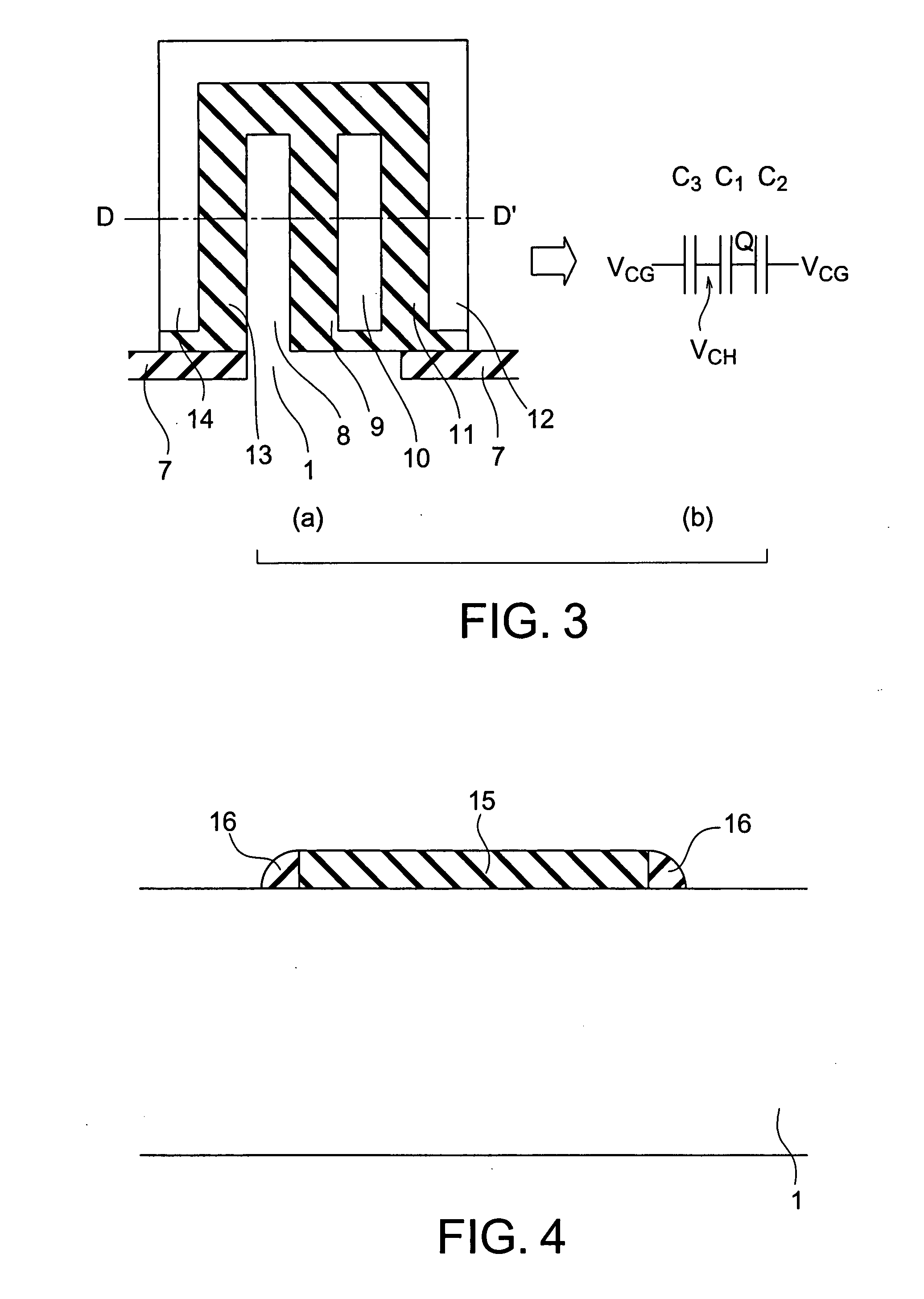
[0027]A nonvolatile semiconductor memory element in accordance with a first embodiment of the present invention includes a charge accumulating layer that is formed on one side face of a plate-like semiconductor region serving as a channel region via an insulating film, a first control gate electrode that is formed on the charge accumulating layer via an insulating film, and a second control gate electrode that is formed on the other side face of the plate-like semiconductor region serving as the channel region via an insulating film.

[0028]With such a structure, higher controllability over the threshold voltages than that of a conventional nonvolatile semiconductor memory element can be achieved. This fact is explained in the following.

[0029]To inject charges into a charge accumulating layer or to release charges from the charge accumulating layer, a tunneling current is used. The tunneling current flows through an insulating film existing between a plate-like semiconductor region se...

second embodiment

[0093]FIG. 13 is a schematic view of a nonvolatile semiconductor memory element in accordance with a second embodiment of the present invention. FIG. 14 is a cross-sectional view of the nonvolatile semiconductor memory element, taken along the line E-E′ of FIG. 13. FIG. 15 is a cross-sectional view of the nonvolatile semiconductor memory element, taken along the line F-F′ of FIG. 13.

[0094]The nonvolatile semiconductor memory element of this embodiment is formed on a SOI substrate 25 having a semiconductor layer 24 formed on a supporting semiconductor substrate 22, with an embedded insulating film 23 being interposed in between. The channel region of the element is formed in the semiconductor layer 24 located between device isolating regions 7. A charge accumulating layer 10 is formed on the channel region, with a first insulating film 9 being interposed in between. A second insulating film 11 is formed on the charge accumulating layer 10. Sidewalls 19 are provided for the stack stru...

third embodiment

[0111]Next, a nonvolatile semiconductor memory device in accordance with a third embodiment of the present invention is described.

[0112]FIG. 20 is a circuit diagram of the nonvolatile semiconductor memory device of this embodiment. This nonvolatile semiconductor memory device has nonvolatile semiconductor memory elements of the first embodiment arranged at lattice points. In FIG. 20, each of the nonvolatile semiconductor memory elements of the first embodiment is represented by the diagram shown in FIG. 21. In FIG. 21, the terminals denoted by S and D are the source and drain, respectively, and the terminal denoted by C.G. is the first and second control gate electrodes that are integrally formed. The terminal of the substrate is not shown. In FIG. 20, each of the nonvolatile semiconductor memory elements of the first embodiment is denoted by Tri,j (1≦i≦M, 1≦j≦N).

[0113]In the nonvolatile semiconductor memory elements arranged in the same row, the plate-like semiconductor regions for...


PUM


Abstract

The channel of each nonvolatile semiconductor memory element has a plate-like shape, and a charge accumulating layer is formed on one face of the channel region, with an insulating film being interposed in between. A control gate electrode is then formed on the charge accumulating layer, with another insulating film being interposed in between. Another control gate electrode is formed on the other face of the channel region, with yet another insulating film being interposed in between. The plate-like semiconductor region is designed to have a thickness smaller than twice the largest depletion layer thickness determined by the impurity concentration. In this manner, variations of the threshold voltages varying with the voltage of the control gate electrodes can be made smaller than the minimum value in conventional elements. As a result, nonvolatile semiconductor memory elements that have higher controllability over threshold voltages and can lower the power supply voltage so as to reduce the power consumption can be provided.

Description

CROSS-REFERENCE TO RELATED APPLICATION[0001]This application is based upon and claims the benefit of priority from prior Japanese Patent Application No. 2006-260931 filed on Sep. 26, 2006 in Japan, the entire contents of which are incorporated herein by reference.BACKGROUND OF THE INVENTION[0002]1. Field of the Invention[0003]The present invention relates to nonvolatile semiconductor memory elements and a nonvolatile semiconductor memory device including the nonvolatile semiconductor memory elements.[0004]2. Related Art[0005]In a conventional nonvolatile semiconductor memory element, the potentials of the control gate electrode and the source / drain regions are controlled, so that charge injection into or charge release from the charge accumulating layer provided between the channel region and the control gate electrode is caused. In this manner, the charge amount in the charge accumulating layer is adjusted, so as to switch the threshold voltages of the element (or the control gate ...

Claims


Application Information

Patent Timeline
IPC IPC(8): H01L29/788
CPCG11C16/0483H01L21/28273H01L27/115H01L29/7881H01L29/42324H01L29/785H01L27/11521H01L29/40114H10B69/00H10B41/30H10B99/00
Inventor ONO, MIZUKI
Owner KK TOSHIBA
Why Eureka
Try Eureka