Thermal processing apparatus and thermal processing method through light irradiation

a technology of thermal processing apparatus and thermal processing method, which is applied in the direction of optical radiation measurement, semiconductor/solid-state device testing/measurement, instruments, etc., can solve the problems of encumbrance of radiation thermometers and excessive output of lamps, and achieve the effect of accurately measuring the temperature of substrates

Inactive Publication Date: 2017-06-22
DAINIPPON SCREEN MTG CO LTD
View PDF14 Cites 11 Cited by
  • Summary
  • Abstract
  • Description
  • Claims
  • Application Information

AI Technical Summary

Benefits of technology

[0025]Therefore, it is an object of the present invention to accurately measure th...

Problems solved by technology

However, when thermal processing of a semiconductor wafer is performed in ammonia atmosphere, temperature measurement by a radiation thermometer is encumbered by ammonia.
Thus, when the ...

Method used


Image

  • Thermal processing apparatus and thermal processing method through light irradiation
  • Thermal processing apparatus and thermal processing method through light irradiation
  • Thermal processing apparatus and thermal processing method through light irradiation

Examples


Embodiment Construction

[0037]Preferred embodiments of the present invention will be described in detail below with reference to the accompanying drawings.

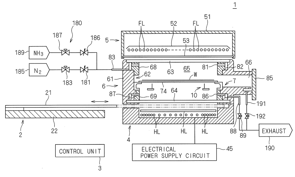
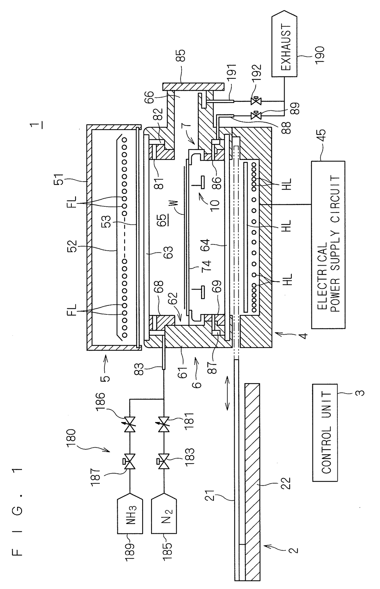
[0038]FIG. 1 is a vertical sectional view illustrating the configuration of a thermal processing apparatus 1 according to the present invention. The thermal processing apparatus 1 according to the present preferred embodiment is a flash lamp annealer configured to facilitate post deposition annealing (PDA) of a high-dielectric-constant gate insulating film (high-k film) by irradiating, with flash light in ammonia atmosphere, a semiconductor substrate W on which the high-dielectric-constant gate insulating film is deposited. In FIG. 1 and the following drawings, the dimension of each component and the number thereof are exaggerated or simplified as necessary to facilitate understanding.

[0039]The thermal processing apparatus 1 includes a chamber 6 configured to house the substrate W, a flash heating unit 5 including a plurality of built-in flash lamps FL, ...


PUM


Abstract

A substrate in a chamber is preheated through light irradiation by a halogen lamp and then heated through irradiation with flash light from a flash lamp. Ammonia is supplied to the chamber from an ammonia supply mechanism to form ammonia atmosphere. The temperature of the substrate at heating processing is measured by a radiation thermometer. When the measurement wavelength band of the radiation thermometer overlaps with the absorption wavelength band of ammonia, the set emissivity of the radiation thermometer is changed and set to be lower than the actual emissivity of the substrate. When radiation light emitted from the substrate is absorbed by the ammonia atmosphere, the radiation thermometer can accurately output the temperature of the substrate as a measured value by reducing the set emissivity of the radiation thermometer.

Description

BACKGROUND OF THE INVENTION[0001]Field of the Invention[0002]The present invention relates to a thermal processing apparatus and a thermal processing method that heat a thin-plate fine electronic substrate (hereinafter simply referred to as a “substrate”) such as a semiconductor wafer by irradiating the substrate with light.[0003]Description of the Background Art[0004]In a process of manufacturing a semiconductor device, flash lamp annealing (FLA) that heats a semiconductor wafer in an extremely short time has attracted attention. The flash lamp annealing is a thermal processing technology of rising temperature only at the surface of a semiconductor wafer in an extremely short time (several milliseconds or less) by irradiating the surface of the semiconductor wafer with flash light using a xenon flash lamp (hereinafter, a simple notation of “flash lamp” means the xenon flash lamp).[0005]The xenon flash lamp has an emission spectral distribution ranging from ultraviolet to near-infra...

Claims


Application Information

Patent Timeline
IPC IPC(8): H01L21/66H01L21/324H05B1/02G01J5/00
CPCH01L22/20G01J5/0007H05B1/0233H01L21/324H01L22/12H01L22/10H01L21/67115H01L21/67248
Inventor FURUKAWA, MASASHIKAWARAZAKI, HIKARUFUSE, KAZUHIKO
Owner DAINIPPON SCREEN MTG CO LTD
Why Eureka
Try Eureka