Imaging device manufacturing method

a manufacturing method and imaging device technology, applied in the direction of diodes, radiation controlled devices, semiconductor devices, etc., can solve the problems of achieve the effect of improving reliability and manufacturing yield, reducing reliability and manufacturing yield

Active Publication Date: 2017-06-22
CANON KK
View PDF1 Cites 1 Cited by
  • Summary
  • Abstract
  • Description
  • Claims
  • Application Information

AI Technical Summary

Benefits of technology

[0008]The present inventors have found that an interlayer insulating film or the like formed on the front surface side of a substrate by a plasma CVD method causes dielectric breakdown to occur in a transistor gate insulating film for an imaging device having a polysilicon film and an insulating film for gettering disposed on the back surface side of the substrate. This may, as a result thereof, reduce reliability and manufacturing yield. The present disclosure is directed to an imaging device manufacturing method capable of contributing to improved reliability and manufacturing yield.

Problems solved by technology

This may, as a result thereof, reduce reliability and manufacturing yield.

Method used


Image

  • Imaging device manufacturing method
  • Imaging device manufacturing method
  • Imaging device manufacturing method

Examples


Embodiment Construction

[0020]Exemplary embodiments of an imaging device manufacturing method will be described in detail below with reference to the attached drawings.

[0021]An imaging device manufacturing method according to a first exemplary embodiment will be described with reference to FIGS. 1A to 7B.

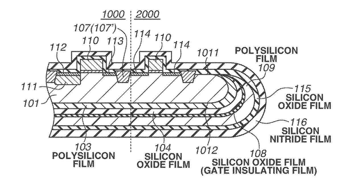
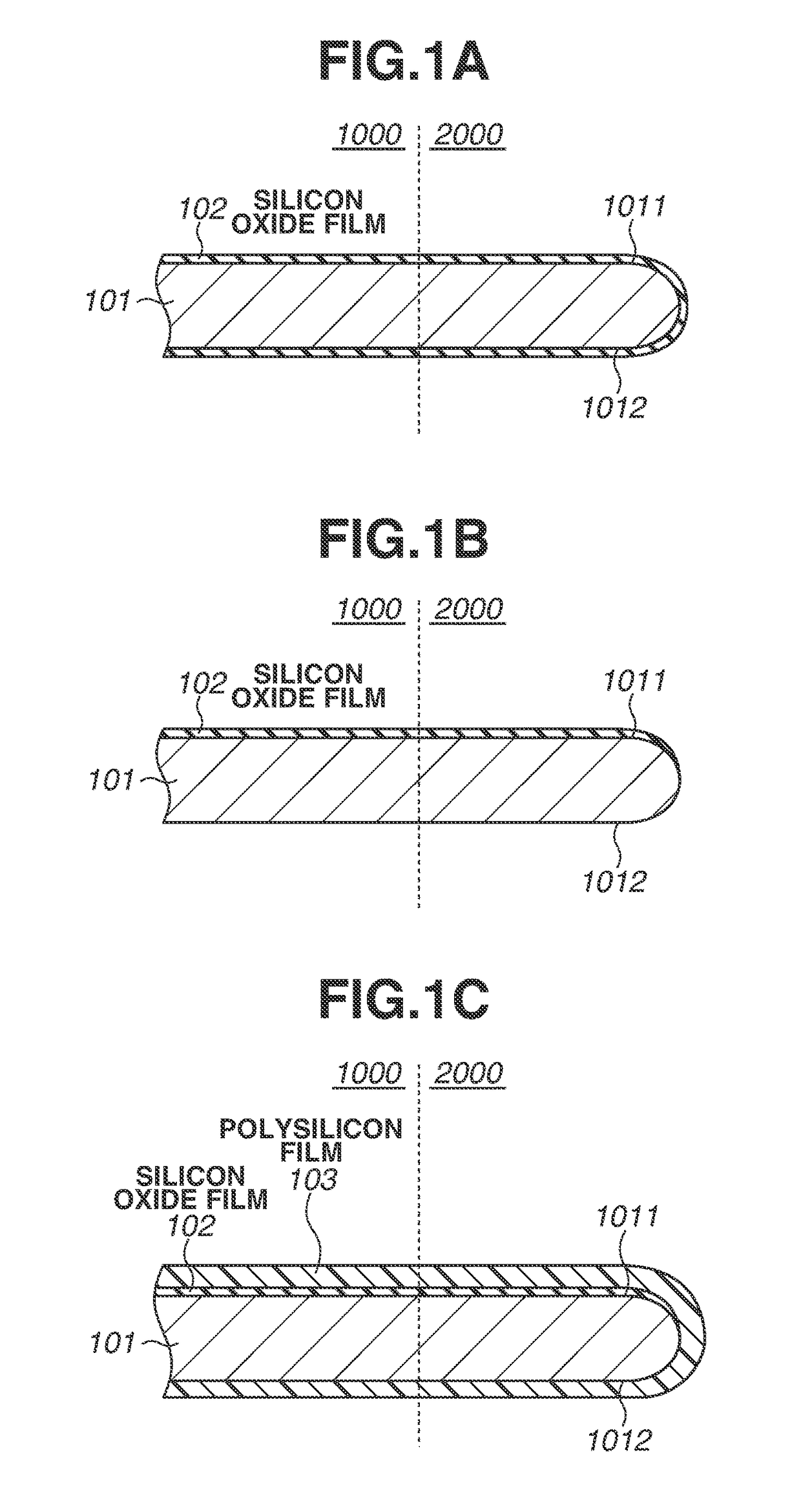
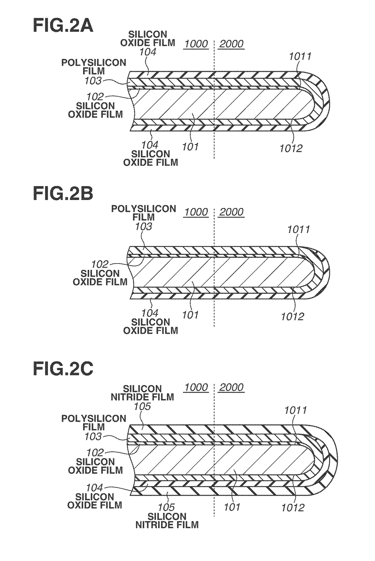
[0022]FIGS. 1A, 1B, and 1C are views schematically illustrating a pixel region 1000 including a photoelectric conversion unit and a plurality of transistors such as transfer transistors, amplifying transistors, and selection transistors. Also schematically illustrated is a peripheral circuit region 2000 disposed outside the pixel region and including a plurality of transistors for processing signals output from the pixel region.

[0023]First, in a process illustrated in FIG. 1A, a silicon substrate 101 including a first main surface 1011 (front surface 1011) and a second main surface 1012 (back surface 1012) is prepared. As used herein, the front surface 1011 is a surface on which a plurality of transistors ...


PUM


Abstract

There is provided an imaging device manufacturing method contributing to improved reliability and yield. The method includes forming a first insulating film on a polysilicon film and then removing a portion of the first insulating film formed on a second main surface and a portion of the first insulating film formed on a side surface of the substrate to expose a polysilicon film. After the polysilicon film is exposed, a second insulating film is formed on the first main surface by a plasma chemical vapor deposition (CVD) method.

Description

BACKGROUND OF THE INVENTION[0001]Field of the Invention[0002]The present disclosure relates to an imaging device manufacturing method.[0003]Description of the Related Art[0004]Metal impurities such as iron and nickel may be mixed into a substrate for an imaging device such as a complementary metal-oxide semiconductor (CMOS) sensor in a process of manufacturing the imaging device. The metal impurities, particularly heavy metal impurities, electrically activated in the silicon substrate may cause white flaws as one of the characteristics of the imaging device due to the fixed charge.[0005]Japanese Patent Application Laid-Open No. 2012-129312 discusses a process of directly forming a polysilicon film on a lower surface of a substrate. The polysilicon film formed on the back surface of the silicon substrate functions as a film for capturing (gettering) the metal impurities mixed in the process of manufacturing the imaging device in a region away from an active region.[0006]In addition, ...

Claims


Application Information

Patent Timeline
Patent Type & Authority Applications(United States)
IPC IPC(8): H01L27/146
CPCH01L27/14689H01L27/14614H01L27/14643H01L27/14692
Inventor HIROTA, KATSUNORIOGAWA, SATOSHIUKIGAYA, NOBUTAKA
Owner CANON KK
Why Eureka
Try Eureka