Method for producing organic semiconductor film and organic transistor

Inactive Publication Date: 2017-06-22
FUJIFILM CORP
View PDF1 Cites 5 Cited by
  • Summary
  • Abstract
  • Description
  • Claims
  • Application Information

AI Technical Summary

Benefits of technology

[0027]According to the present invention, it is possible to provide a method for producing an o

Problems solved by technology

When the present inventors have produced an organic semiconductor film by the method disclosed in JP2011-258824A using the organic semiconductor solution disclosed in the document, the size of the

Method used


Image

  • Method for producing organic semiconductor film and organic transistor
  • Method for producing organic semiconductor film and organic transistor
  • Method for producing organic semiconductor film and organic transistor

Examples


Example

Modification Example 1

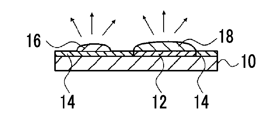
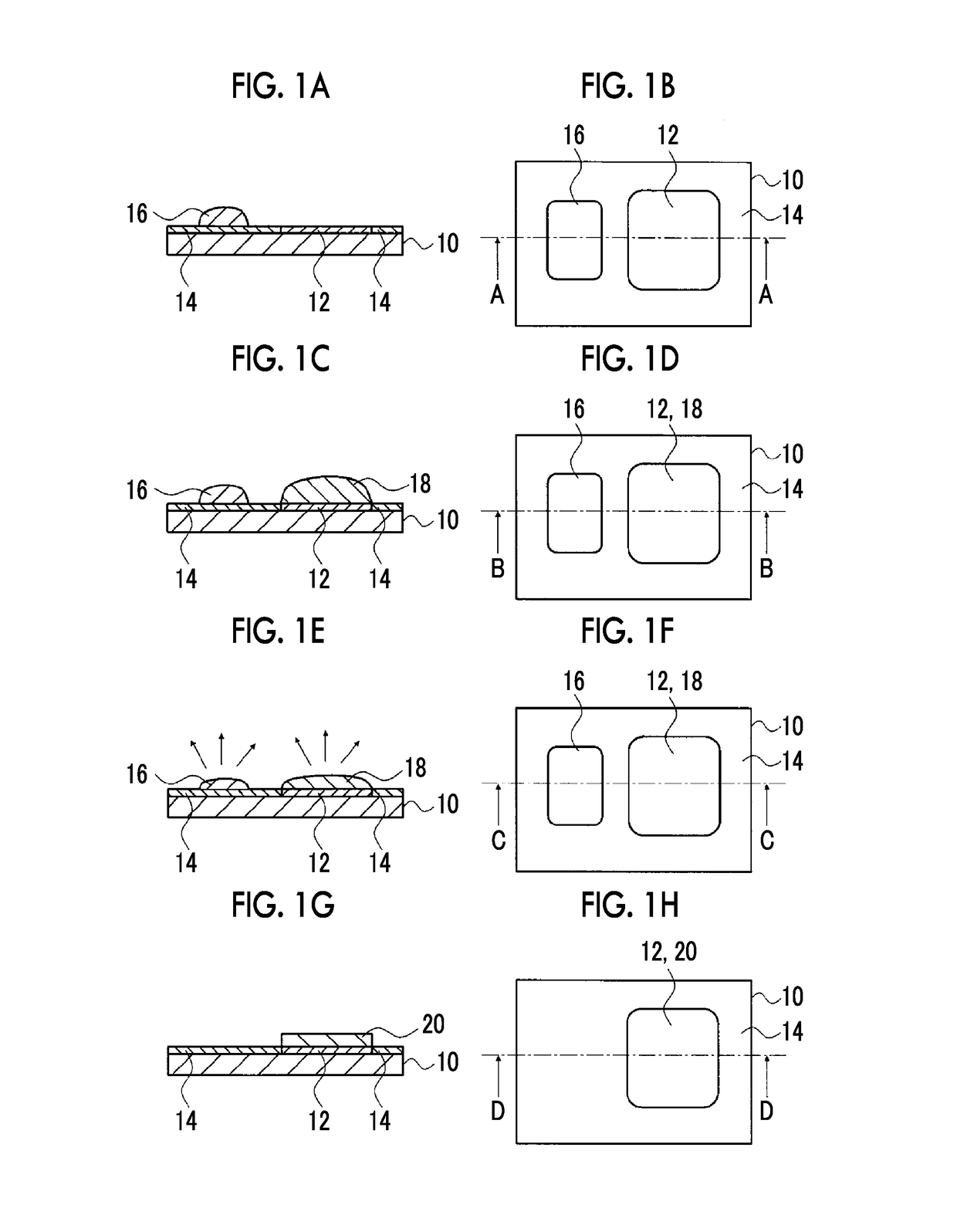
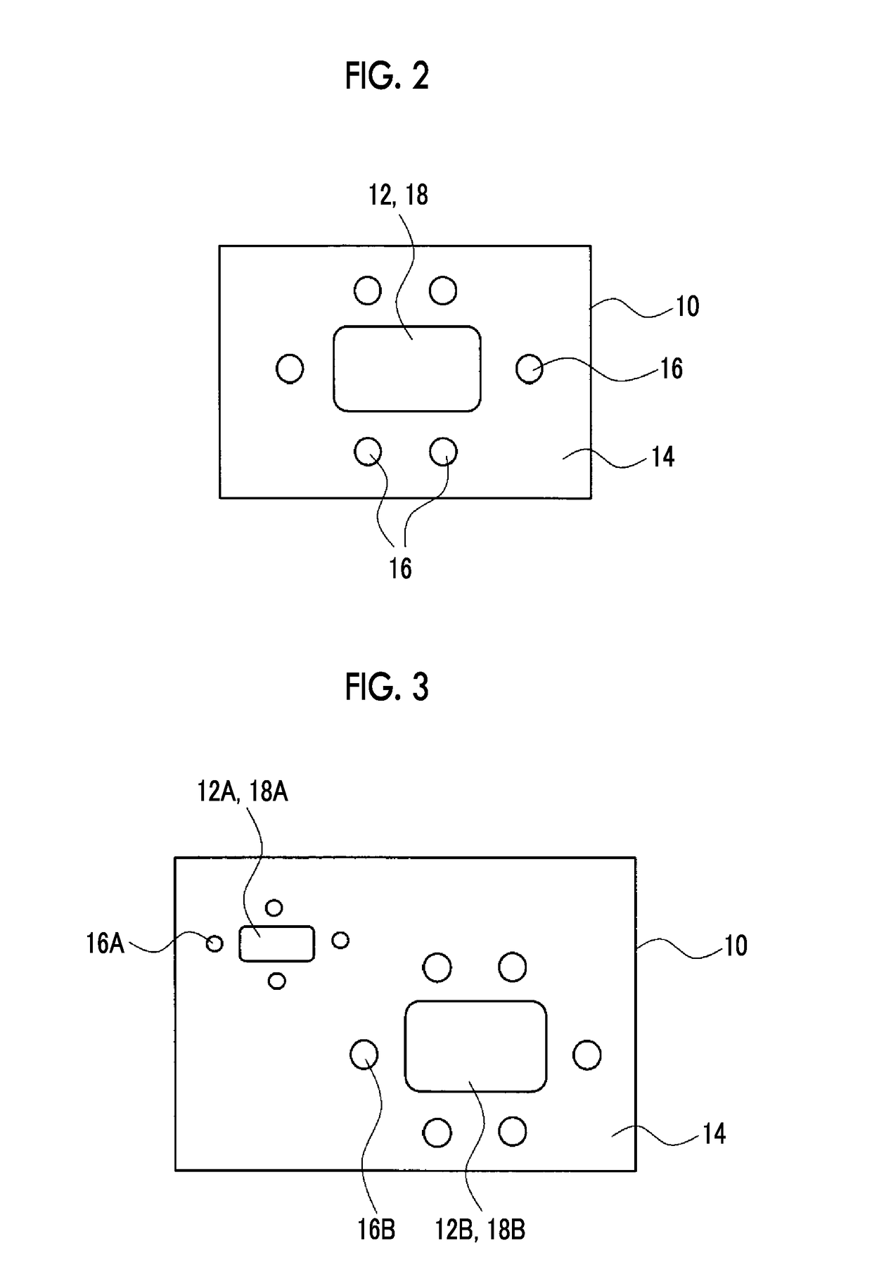
[0111]In FIGS. 1A to 1H, an embodiment in which the solvent 16 for volatilization rate control is applied to one location in the liquid repellent region 14 has been described in Step B but the present invention is not limited to the embodiment. The solvent for volatilization rate control may be applied to a plurality of locations in the liquid repellent region so as to surround the lyophilic region. Specifically, as shown in FIG. 2, the ink 18 is applied to the lyophilic region 12 on the substrate 10 and also the solvent 16 for volatilization rate control may be applied to a plurality of locations in the liquid repellent region 14 (at six locations in FIG. 2) so as to surround the lyophilic region 12. By applying the solvent for volatilization rate control to a plurality of locations as described above, the volatilization rate of the first solvent in the ink is easily controlled and the effect of the present invention is further enhanced.

[0112]The position to w...

Example

Modification Example 2

[0115]As described above, the pattern of the lyophilic region and the liquid repellent region formed on the substrate are not particularly limited. For example, a plurality of lyophilic regions may be formed and the sizes (area) and shapes of the plurality of lyophilic regions may be different from each other.

[0116]In Step B, the amount, position, and number of locations of the solvent for volatilization rate control applied in the liquid repellent region may be adjusted according to the size (area) and shape of the lyophilic region. That is, when the solvent for volatilization rate control is applied to the liquid repellent region in the vicinity of the lyophilic region on the substrate having the plurality of lyophilic regions in which at least one of size or shape is different (size and / or shape is different) and the liquid repellent region, according to the sizes and / or shapes of the respective lyophilic regions, at least one of the amount, position, or num...

Example

Modification Example 3

[0118]As described above, the shape of the lyophilic region is not particularly limited and various shapes may be adopted.

[0119]Among these, from the viewpoint of further enhancing the effect of the present invention, the lyophilic region preferably has an ink accumulation region and an ink narrowing region (seed crystal precipitation region) connected to the ink accumulation region and having a narrower width than that of the ink accumulation region. More specifically, as shown in FIG. 4, a lyophilic region 120 and a liquid repellent region 14 are disposed on a substrate 100 and the lyophilic region 120 has an ink accumulation region 22 and an ink narrowing region 24.

[0120]When the ink is applied to the lyophilic region having two regions as described above, the ink in the ink narrowing region has a narrower width that that of the other region and thus, the solvents (the first solvent and the second solvent) included in the ink easily volatilize. Therefore, an...


PUM


Abstract

A method for producing an organic semiconductor film includes performing, in random order, applying an ink including an organic semiconductor, a first solvent having high affinity for the organic semiconductor, and a second solvent having lower affinity for the organic semiconductor than the first solvent and having a higher boiling point than the first solvent, to a lyophilic region of a substrate having at least one of a lyophilic region or a liquid repellent region disposed in the vicinity of the lyophilic region on a surface, and applying a solvent composed of the same type of solvent as the first solvent and used for controlling a volatilization rate of the first solvent in the ink applied to the lyophilic or the liquid repellant region; and then causing the first and second solvent in the ink applied to the lyophilic region to volatilize to produce an organic semiconductor film.

Description

CROSS-REFERENCE TO RELATED APPLICATIONS[0001]This application is a Continuation of PCT International Application No. PCT / JP2015 / 072925 filed on Aug. 13, 2015, which claims priority under 35 U.S.C. §119(a) to Japanese Patent Application No. 2014-199122 filed on Sep. 29, 2014. The above application is hereby expressly incorporated by reference, in its entirety, into the present application.BACKGROUND OF THE INVENTION[0002]1. Field of the Invention[0003]The present invention relates to a method for producing an organic semiconductor film and an organic transistor.[0004]2. Description of the Related Art[0005]Since weight reduction, cost reduction and flexibility can be achieved, an organic thin film transistor (organic TFT) is used for liquid crystal displays, organic electro luminescence (EL) displays, radio frequency identifiers (RFID), and the like.[0006]In the production of an organic thin film transistor, there is a possibility that an organic semiconductor film having a large area...

Claims


Application Information

Patent Timeline
IPC IPC(8): H01L51/00
CPCH01L51/0007H01L51/0005H01L51/0558H01L51/0096H01L51/0012Y02E10/549Y02P70/50H10K71/15H10K71/135H10K77/10H10K10/484H10K71/191
Inventor OHTA, HIROSHI
Owner FUJIFILM CORP
Why Eureka
Try Eureka