Pixel circuit of active-matrix light-emitting diode and display panel having the same

Inactive Publication Date: 2017-06-29
INNOLUX CORP
View PDF17 Cites 30 Cited by
  • Summary
  • Abstract
  • Description
  • Claims
  • Application Information

AI Technical Summary

Benefits of technology

[0008]The object of the present disclosure is to provide a pixel circuit of active-matrix light-emitting diode and a display panel having the same, in which the light-emitting transistor of the pixel circuit is a polysilicon transistor that has a large current in its turn-on state thereby providing a large driving capability to drive the light-emitting diode. Furthermore, the driving transistor of the pixel circuit is an oxide semiconductor transistor that has a relativel

Problems solved by technology

For the known N-type driving transistor (NTFT_dri), it may suffer a problem of threshold voltage variation.
Accordingly, when driving voltages with the same value are respectively in

Method used


Image

  • Pixel circuit of active-matrix light-emitting diode and display panel having the same
  • Pixel circuit of active-matrix light-emitting diode and display panel having the same
  • Pixel circuit of active-matrix light-emitting diode and display panel having the same

Examples


first embodiment

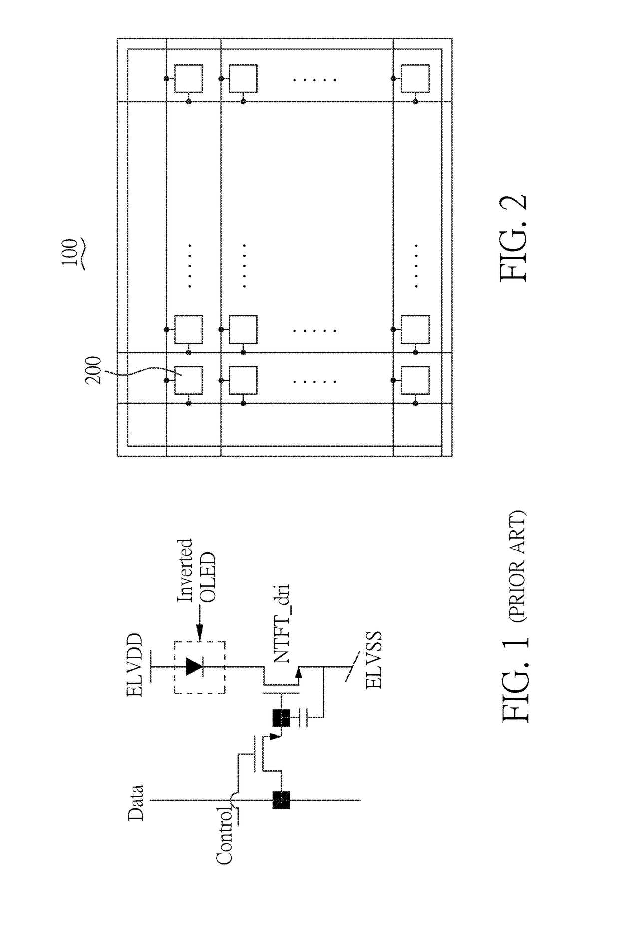
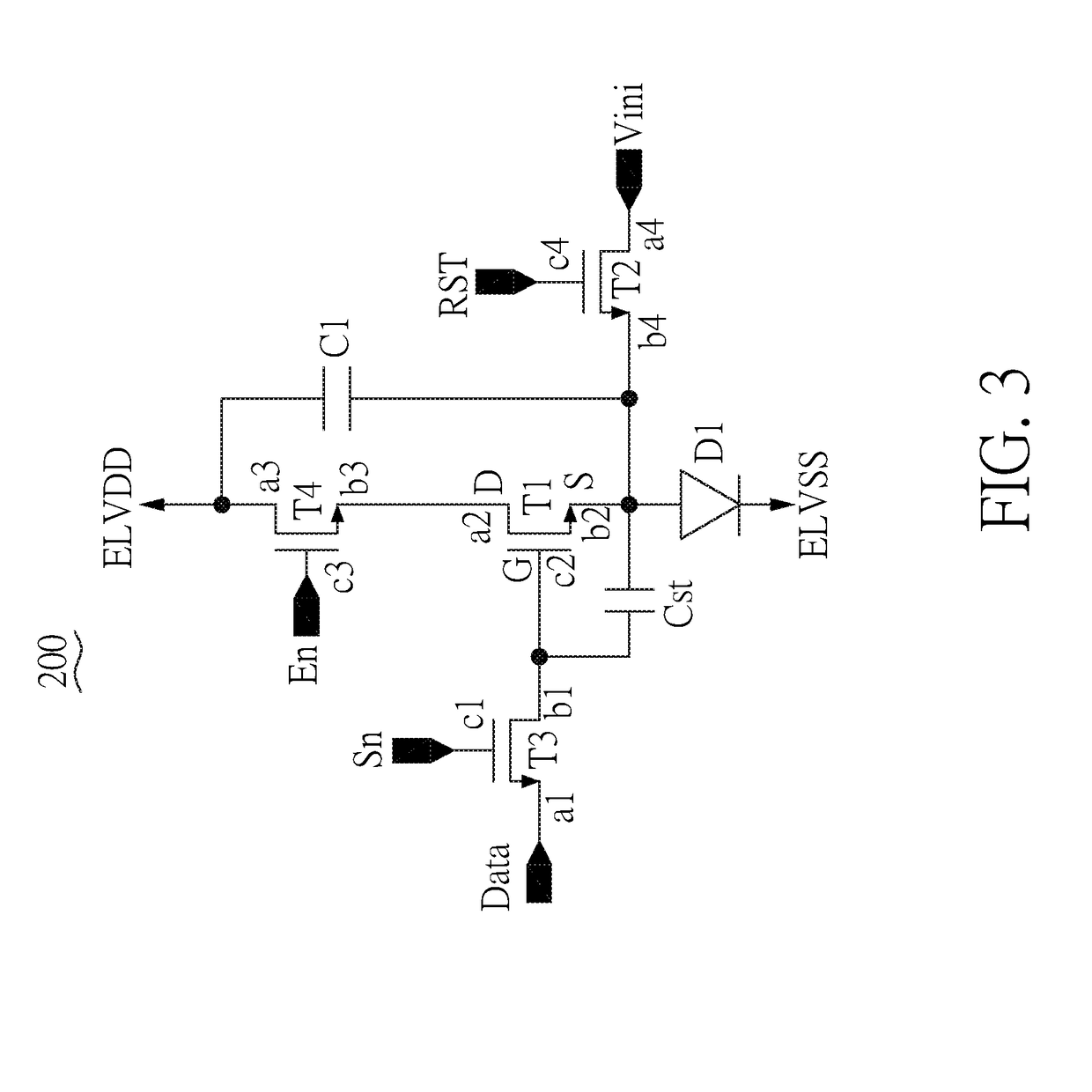
[0081]In another embodiment, FIG. 2 is a schematic diagram of a display panel according to the present disclosure. The display panel 100 is an light-emitting diode display panel having a plurality of pixel circuits 200 of active-matrix light-emitting diode, where the light emitting diode (D1) can be an organic light emitting diode or a LED chip. Each of the pixel circuits 200 is used to drive a corresponding device for display. FIG. 3 is a circuit diagram of a pixel circuit 200 of active-matrix light-emitting diode according to the present disclosure. As shown in FIG. 3, the pixel circuit 200 includes a third transistor (T3), a first transistor (T1), a first storage capacitor (Cst), a fourth transistor (T4), a second storage capacitor (C1), and a second transistor (T2). The pixel circuit 200 is used to drive a light-emitting diode (D1).

[0082]The third transistor (T3) has a second control terminal (c1) connected to a first control signal (Sn), a fourth terminal (a1) connected to a da...

second embodiment

[0104]FIG. 12 is a circuit diagram of active-matrix light-emitting diode according to the present disclosure. In comparison with FIG. 3, the pixel circuit 200 in FIG. 12 further comprises a fifth transistor (T5). The fifth transistor (T5) has a fifth control terminal (c5) connected to a compensated / sensing signal, a tenth terminal (a5) connected to a compensated / sensing line, and an eleventh terminal (b5) connected to the third terminal (b2). The connection for the remaining components is similar to that for FIG. 3, and therefore is not repeated again.

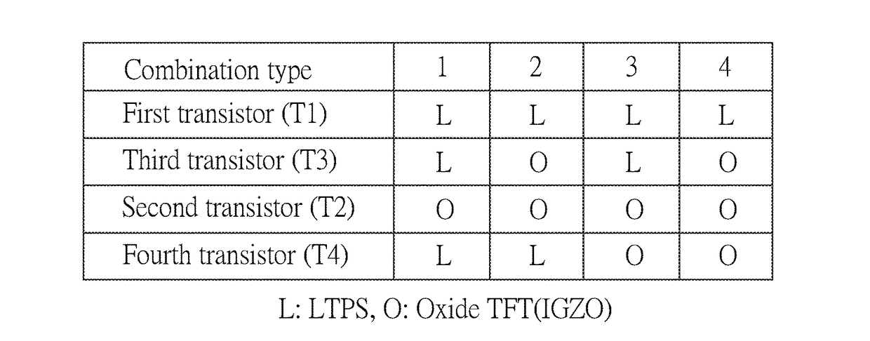
[0105]As shown in FIG. 12, the fourth transistor (T4) is a transistor comprising a polysilicon semiconductor layer, the first transistor (T1) is a transistor comprising an oxide semiconductor layer, and the third transistor (T3), the second transistor (T2) and the fifth transistor (T5) are each a transistor comprising the polysilicon semiconductor layer or a transistor comprising the oxide semiconductor layer.

[0106]FIG. 13 is schematic...

third embodiment

[0109]FIG. 16 is a circuit diagram of a pixel circuit 200 of active-matrix light-emitting diode according to the present disclosure. In comparison with FIG. 12, the fifth transistor (T5) in FIG. 16 has a fifth control terminal (c5) connected to the compensated / sensing signal, a tenth terminal (a5) connected to the data line (Data), and an eleventh terminal (b5) connected to the third terminal (b2). The connection for the remaining components is similar to that for FIG. 12, and therefore is not repeated again.

[0110]FIG. 17 is schematic view illustrating an application of the pixel circuit 200 of FIG. 16 according to the present disclosure, which is similar to FIG. 16 except that, in FIG. 17, the compensated / sensing signal of the pixel circuit 200 is removed, and the fifth control terminal (c5) is connected to the second control signal (En). In this example, the fourth transistor (T4) is a P-type transistor, and the fifth transistor (T5) is an N-type transistor.

[0111]FIG. 18 is schema...


PUM


Abstract

A display includes a pixel circuit. The pixel circuit includes a light emitting diode, a first transistor, a second transistor and a third transistor. The first transistor includes a first semiconductor layer. The first transistor has a first control terminal, a second terminal, and a third terminal electrically connected to the light emitting diode. The second transistor includes a second semiconductor layer, and is electrically connected to the third terminal. The third transistor is electrically connected to the first control terminal. A material of the first semiconductor layer is different from a material of the second semiconductor layer.

Description

BACKGROUND[0001]1. Field of the Disclosure[0002]The present disclosure relates to the technical field of liquid crystal display panels and, more particularly, to a pixel circuit of active-matrix light-emitting diode and a display panel having the same.[0003]2. Description of Related Art[0004]Typically, based on the substrate manufacturing process, the type of driving transistor for active-matrix light-emitting diode pixel can be divided into P-type and N-type. FIG. 1 is a 2T1C pixel circuit with an N-type driving transistor, which is used to drive an inverted light-emitting diode.[0005]The N-type driving transistor (NTFT_dri) has a gate / source voltage (Vgs) that corresponds to a data level and a low level (ELVSS). For the known N-type driving transistor (NTFT_dri), it may suffer a problem of threshold voltage variation. That is, due to the polycrystalline process, the threshold voltages Vt of different N-type driving transistors are varied owing to different locations of the N-type ...

Claims


Application Information

Patent Timeline
IPC IPC(8): H01L27/12H01L29/417
CPCH01L27/1251H01L27/1225H01L29/41733H01L27/1248H01L27/124H01L29/7869G09G3/3258H01L27/3262H01L25/167G09G2320/0233G09G3/3233G09G2300/0852H01L29/78675G09G2300/0819G09G2300/0842G09G2300/0861G09G2310/0262H01L27/1229H10K59/1213
Inventor LEE, KUANFENGKUO, KUNG-CHENCHEN, LIEN-HSIANGTSAI, YU-SHENG
Owner INNOLUX CORP
Why Eureka
Try Eureka