Electrostatic discharge protection device and operation method thereof

Active Publication Date: 2017-07-06
NOVATEK MICROELECTRONICS CORP
10 Cites 4 Cited by

AI-Extracted Technical Summary

Problems solved by technology

However, while the ESD protection device is applied to the high-frequency circuits, the parasitic capacitance of the ESD pr...

Benefits of technology

[0004]The disclosure is directed to an electrostatic discharge (ESD) protection device and an opera...

Abstract

An electrostatic discharge (ESD) protection device and an operation method of the ESD protection device are provided. The ESD protection device includes an ESD current rail, an ESD protection element string, and a bias circuit. A first end and a second end of the ESD protection element string are electrically connected to the ESD current rail and a signal pad, respectively. The ESD protection element string includes a first ESD protection element and a second ESD protection element that are serially connected. The bias circuit is electrically connected to the ESD protection element string to provide a bias voltage to a common connection node between the first ESD protection element and the second ESD protection element.

Application Domain

Semiconductor/solid-state device detailsEmergency protective arrangements for limiting excess voltage/current

Technology Topic

Electrostatic discharge protectionElectricity +1

Image

  • Electrostatic discharge protection device and operation method thereof
  • Electrostatic discharge protection device and operation method thereof
  • Electrostatic discharge protection device and operation method thereof

Examples

  • Experimental program(1)

Example

[0029]The term “coupled (or connected)” used in this disclosure (including claims) may express any direct or indirect connection means. For instance, “a first apparatus is coupled (or connected) to a second apparatus” should be interpreted as “the first apparatus is directly connected to the second apparatus” or “the first apparatus is indirectly connected to the second apparatus through other apparatuses or connection means.” Moreover, wherever appropriate, elements/components/steps with the same reference numerals in the drawings and embodiments represent the same or similar parts. Elements/components/steps with the same reference numerals or names in different embodiments may be cross-referenced.
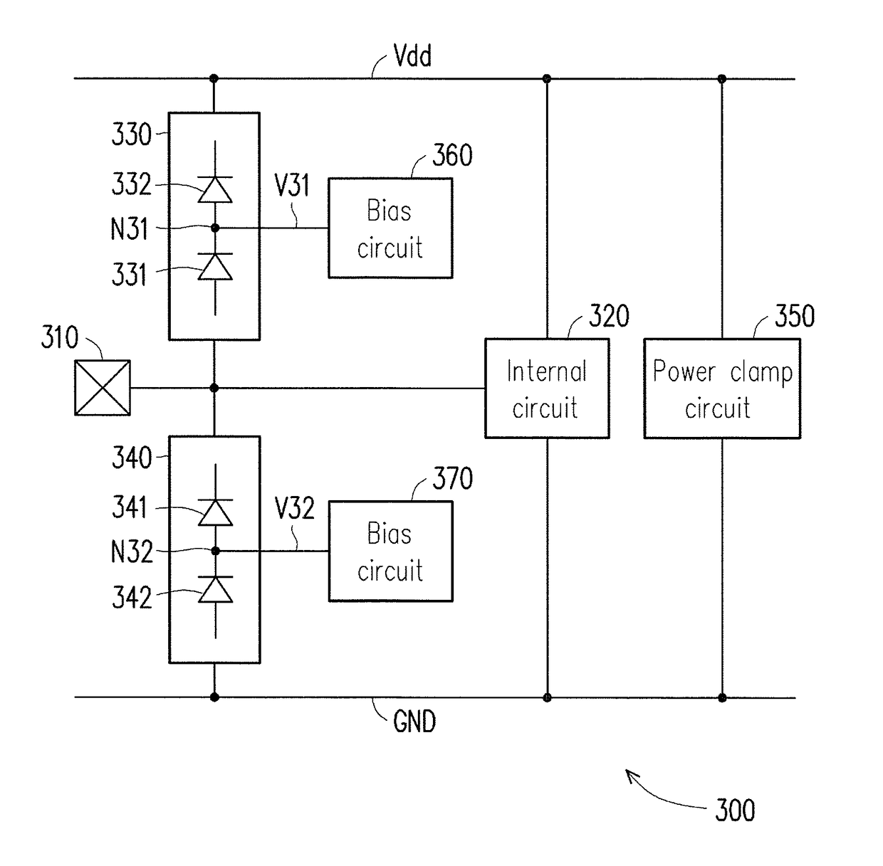
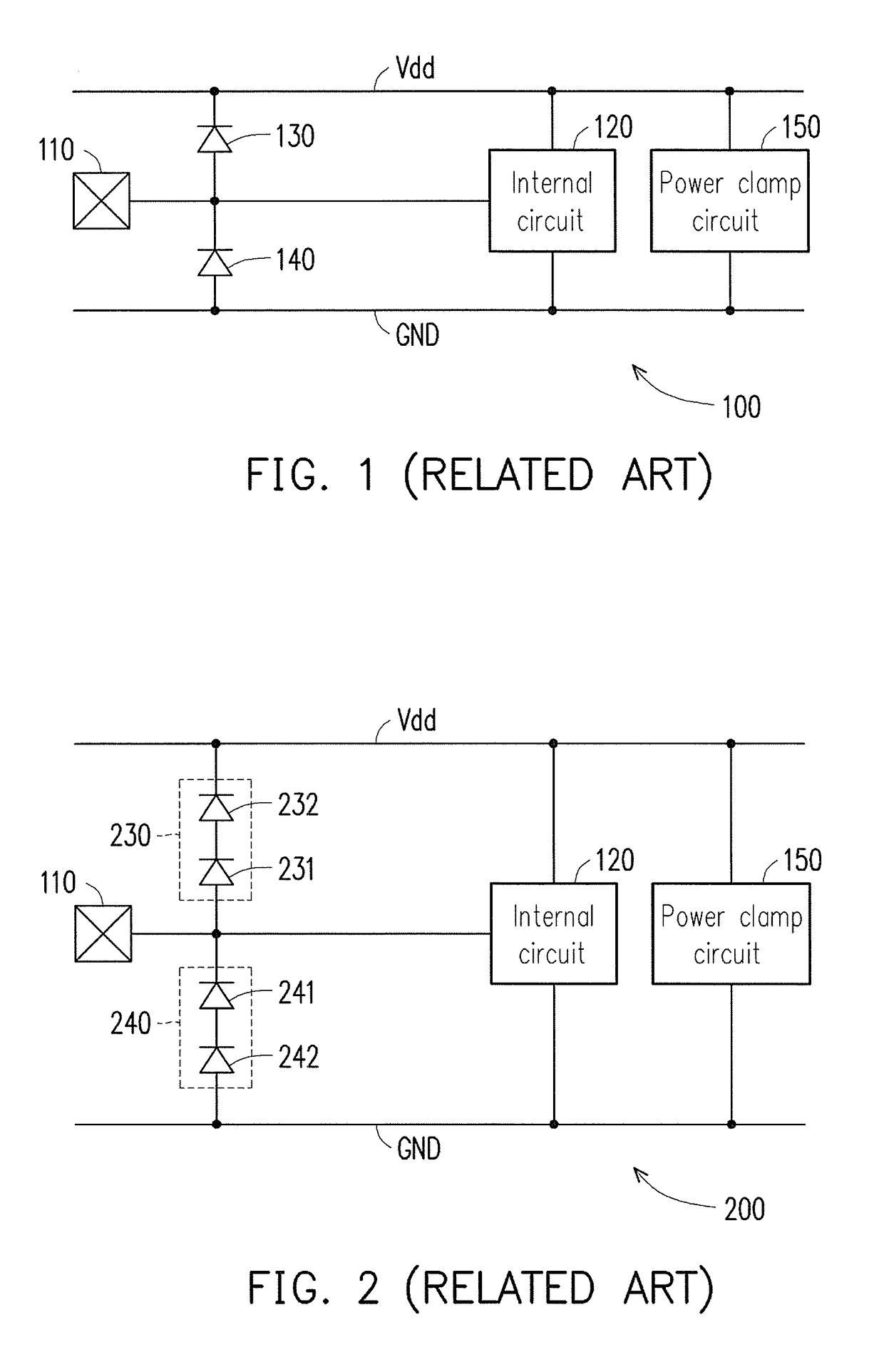
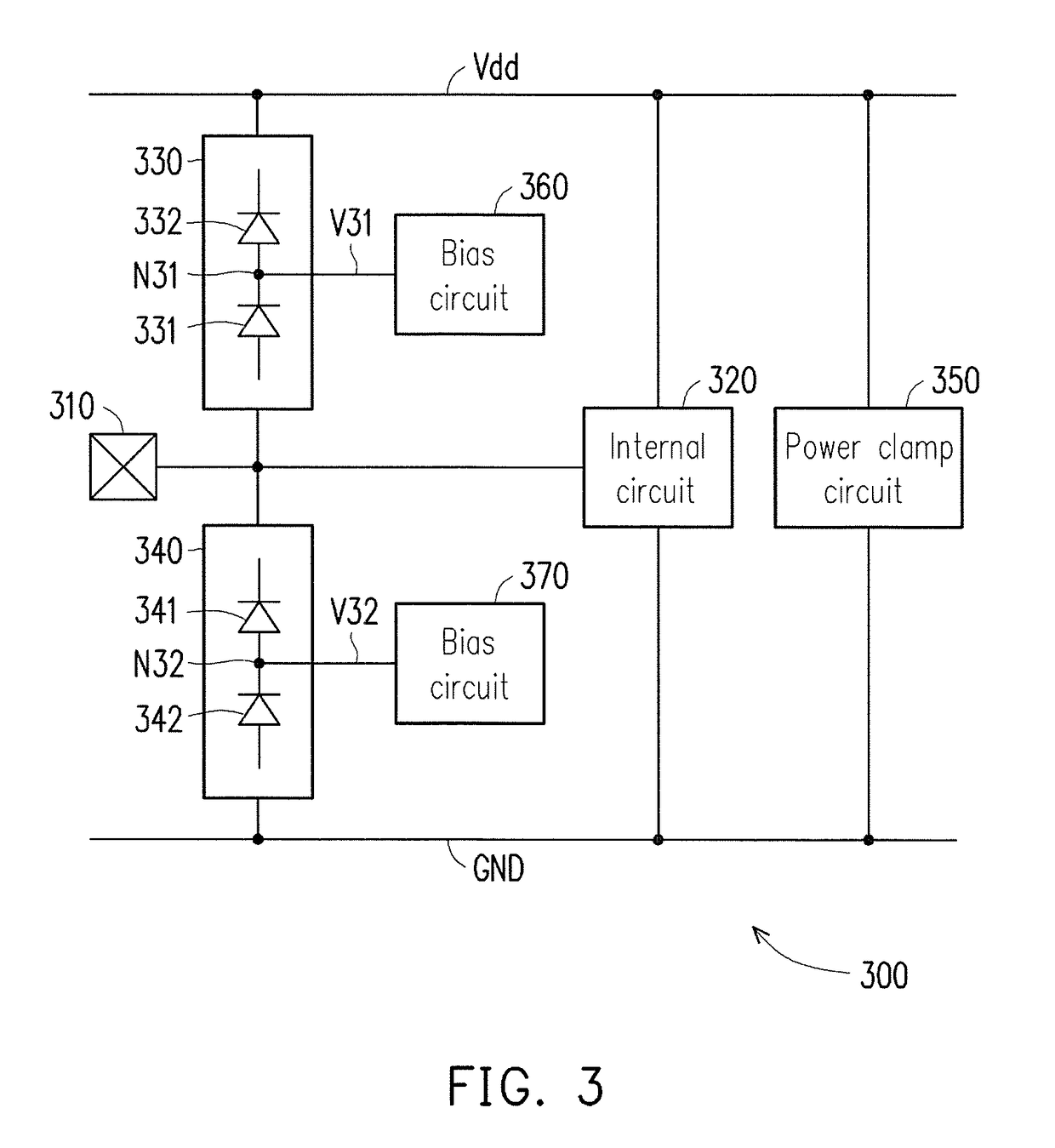
[0030]FIG. 1 is a schematic block circuit diagram of a conventional integrated circuit 100. The integrated circuit 100 includes a signal pad 110, an internal circuit 120, a diode 130, a diode 140, a supply voltage rail Vdd, a ground voltage rail GND, and a power clamp circuit 150. The signal pad 110 is coupled to the internal circuit 120. The internal circuit 120 stands for a core circuit and/or a functional circuit of the integrated circuit 100. The cathode of the diode (i.e., the ESD protection element) is electrically connected to the supply voltage rail Vdd. The anode of the diode 130 is electrically connected to the signal pad 110. The cathode of the diode 140 (i.e., the ESD protection element) is electrically connected to the signal pad 110. The anode of the diode 140 is electrically connected to the ground voltage rail GND. The power clamp circuit 150 is electrically connected between the supply voltage rail Vdd and the ground voltage rail GND. Since the power clamp circuit 150 may be a conventional ESD clamp circuit, no explanation will be further provided hereinafter.
[0031]When an ESD positive pulse arrives at the signal pad 110, the ESD current may be guided to the supply voltage rail Vdd through the diode 130; alternatively, the ESD current may be guided to the ground voltage rail GND through the diode 130, the supply voltage rail Vdd, and the power clamp circuit 150. When an ESD negative pulse arrives at the signal pad 110, the ESD current may be guided to the signal pad 110 from the ground voltage rail GND through the diode 140; alternatively, the ESD current may be guided to the signal pad 110 from the supply voltage rail Vdd through the power clamp 150, the ground voltage rail GND, and the diode 140. Thereby, the internal circuit 120 may be protected from being burnt down by the ESD current. The FIG. 1 has been described above with reference to “ESD protection design for 900-MHz RF receiver with 8-kV HBM ESD robustness” (M.-D. Ker, W.-Y. Lo, C.-M. Lee, C.-P. Chen, and H.-S. Kao, in IEEE Radio Frequency Integrated Circuits Symp. Dig., 2002, pp. 427-430).
[0032]FIG. 2 is a schematic block circuit diagram of another conventional integrated circuit 200. The integrated circuit 200 includes a signal pad 110, an internal circuit 120, an ESD protection element string 230, an ESD protection element string 240, a supply voltage rail Vdd, a ground voltage rail GND, and a power clamp circuit 150. The signal pad 110, the internal circuit 120, the supply voltage rail Vdd, the ground voltage rail GND, and the power clamp circuit 150 have been described above with reference to FIG. 1. The ESD protection element string 230 is electrically connected between the supply voltage rail Vdd and the signal pad 110. The ESD protection element string 240 is electrically connected between the signal pad 110 and the ground voltage rail GND. The ESD protection operations of the ESD protection element strings 230 and 240 and the power clamp circuit 150 as shown in FIG. 2 may be deduced from those of the diodes 130 and 140 and the power clamp circuit 150 as shown in FIG. 1, and therefore no description will be further provided hereinafter.
[0033]The ESD protection element string 230 illustrated in FIG. 2 includes diodes 231 and 232. An anode of the diode 231 (i.e., the ESD protection element) is electrically connected to the signal pad 110. A cathode of the diode 231 is electrically connected to an anode of the diode 232 (i.e., the ESD protection element). A cathode of the diode 232 is electrically connected to the supply voltage rail Vdd. The ESD protection element string 240 includes diodes 241 and 242. A cathode of the diode 241 (i.e., the ESD protection element) is electrically connected to the signal pad 110. An anode of the diode 241 is electrically connected to a cathode of the diode 242 (i.e., the ESD protection element). An anode of the diode 242 is electrically connected to the ground voltage rail GND. To simplify the explanation, it is assumed that the properties (e.g., the capacitance of the parasitic capacitor) of the diodes 231, 232, 241, and 242 are identical to those of the diodes 130 and 140 as shown in FIG. 1. The parasitic capacitor of the diode 231 and the parasitic capacitor of the diode 232 are serially connected between the supply voltage rail Vdd and the signal pad 110, such that the capacitance of the parasitic capacitor of the ESD protection element string 230 shown in FIG. 2 is less than the capacitance of the parasitic capacitor of the diode 130 shown in FIG. 1. Specifically, the capacitance of the parasitic capacitor of the ESD protection element string 230 shown in FIG. 2 is half the capacitance of the parasitic capacitor of the diode 130 shown in FIG. 1. In view of the above, the capacitance of the parasitic capacitor of the ESD protection element string 240 shown in FIG. 2 is half the capacitance of the parasitic capacitor of the diode 140 shown in FIG. 1. The FIG. 2 has been described above with reference to “Improving ESD robustness of stacked diodes with embedded SCR for RF applications in 65-nm CMOS” (C.-Y. Lin, M.-L. Fan, M.-D. Ker, L.-W. Chu, J.-C. Tseng, and M.-H. Song, in Proc. IEEE International Reliability Physics Symp., 2014).
[0034]FIG. 3 is a schematic block circuit diagram of an integrated circuit 300 according to an embodiment of the disclosure. The integrated circuit 300 includes a signal pad 310, an internal circuit 320, an ESD protection element string 330, an ESD protection element string 340, a power clamp circuit 350, a bias circuit 360, and a bias circuit 370. Besides, the integrated circuit 300 further includes two ESD current rails, e.g., the supply voltage rail Vdd and the ground voltage rail GND shown in FIG. 3. Descriptions of the signal pad 310, the internal circuit 320, the ESD protection element string 330, the ESD protection element string 340, the supply voltage rail Vdd, the ground voltage rail GND, and the power clamp circuit 350 as shown in FIG. 3 may be deduced from the descriptions of the signal pad 110, the internal circuit 120, the diode 130, the diode 140, the supply voltage rail Vdd, the ground voltage rail GND, and the power clamp circuit 150 as shown in FIG. 1 and/or the descriptions of the signal pad 110, the internal circuit 120, the ESD protection element string 230, the ESD protection element string 240, the supply voltage rail Vdd, the ground voltage rail GND, and the power clamp circuit 150 as shown in FIG. 2, and therefore no other explanations will be further given below.
[0035]With reference to FIG. 3, a first end and a second end of the ESD protection element string 330 are electrically connected to the supply voltage rail Vdd (equivalent to one ESD current rail) and the signal pad 310, respectively. The ESD protection element string 330 includes an ESD protection element 331 and an ESD protection element 332 that are serially connected. A first end and a second end of the ESD protection element string 340 are electrically connected to the ground voltage rail GND (equivalent to the other ESD current rail) and the signal pad 310, respectively. The ESD protection element string 340 includes an ESD protection element 341 and an ESD protection element 342 that are serially connected. In the present embodiment, the ESD protection elements 331, 332, 341, and 342 may be diodes. In other embodiments of the disclosure, the ESD protection elements 331, 332, 341, and/or 342 may be silicon controlled rectifiers (SCR), transistors, or other types of ESD protection elements. The ESD protection operations of the ESD protection element strings 330 and 340 and the power clamp circuit 350 as shown in FIG. 3 may be deduced from those of the diodes 130 and 140 and the power clamp circuit 150 as shown in FIG. 1, and therefore no description will be further provided hereinafter.
[0036]The bias circuit 360 is electrically connected to the ESD protection element string 330 to provide a bias voltage V31 to a common connection node N31 between the ESD protection element 331 and the ESD protection element 332. A voltage of the common connection node N31 is assumed to be an original division voltage Vod31 when the bias circuit 360 is not electrically connected to the ESD protection element string 330. In some embodiments of the disclosure, the bias voltage V31 may be greater than the original division voltage Vod31, such that the voltage drop of the ESD protection element 331 (i.e., the voltage difference between two ends of the ESD protection element 331) may be increased during the normal operation period. In other embodiments of the disclosure, the bias voltage V31 may be less than the original division voltage Vod31, such that the voltage drop of the ESD protection element 332 (i.e., the voltage difference between two ends of the ESD protection element 332) may be increased during the normal operation period.
[0037]The bias circuit 370 is electrically connected to the ESD protection element string 340 to provide a bias voltage V32 to a common connection node N32 between the ESD protection element 341 and the ESD protection element 342. A voltage of the common connection node N32 is assumed to be an original division voltage Vod32 when the bias circuit 370 is not electrically connected to the ESD protection element string 340. In some embodiments of the disclosure, the bias voltage V32 may be greater than the original division voltage Vod32, such that the voltage drop of the ESD protection element 342 (i.e., the voltage difference between two ends of the ESD protection element 342) may be increased during the normal operation period. In other embodiments of the disclosure, the bias voltage V32 may be less than the original division voltage Vod32, such that the voltage drop of the ESD protection element 341 (i.e., the voltage difference between two ends of the ESD protection element 341) may be increased during the normal operation period.
[0038]FIG. 4 is a schematic flowchart illustrating an operation method of an ESD protection device according to an embodiment of the disclosure. With reference to FIG. 3 and FIG. 4, in step S410, the supply voltage rail Vdd (equivalent to one ESD current rail), the ground voltage rail GND (equivalent to the other ESD current rail), the ESD protection element string 330, and the ESD protection element string 340 are provided to the integrated circuit 300. A first end and a second end of the ESD protection element string 330 are electrically connected to the supply voltage rail Vdd and the signal pad 310, respectively, and a first end and a second end of the ESD protection element string 340 are electrically connected to the ground voltage rail GND and the signal pad 310, respectively. The ESD protection element string 330 includes the ESD protection elements 331 and 332 that are serially connected to each other; the ESD protection element string 340 includes the ESD protection elements 341 and 342 that are serially connected to each other. In step S420, the bias circuit 360 provides the bias voltage V31 to the common connection node N31 between the ESD protection elements 331 and 332, and the bias circuit 370 provides the bias voltage V32 to the common connection node N32 between the ESD protection elements 341 and 342.
[0039]FIG. 5 is a schematic curve illustrating properties of voltage drop and parasitic capacitance of a diode. In FIG. 5, the horizontal axis represents the voltage drop of the diode (i.e., the voltage difference between the two ends of the diode in the event that the reverse bias voltage is applied) in the unit of volts; the vertical axis represents the capacitance of the parasitic capacitor of the diode in the unit of femto-farads (fF). The numeric values on the horizontal axis and the vertical axis in FIG. 5 are merely schematic and serve as references. Due to different parameters including materials and manufacturing processes, different diodes may have different capacitances. As shown in FIG. 5, the greater the voltage drop of the diode (i.e., the ESD protection element), the smaller the capacitance of the parasitic capacitor of the diode.
[0040]With reference to FIG. 3, the bias voltage V31 changes the voltage level of the common connection node N31 and further increases the voltage drop of the ESD protection element 331 or the voltage drop of the ESD protection element 332 (i.e., the voltage difference between the two ends of the diode in the event that the reverse bias voltage is given). The greater the voltage drop of the diode (i.e., the ESD protection element), the smaller the capacitance of the parasitic capacitor of the diode. Accordingly, the capacitance of the parasitic capacitor of the ESD protection element string 330 may be reduced. Similarly, the bias voltage V32 changes the voltage level of the common connection node N32 and further increases the voltage drop of the ESD protection element 341 or the voltage drop of the ESD protection element 342 (i.e., the voltage difference between the two ends of the diode in the event that the reverse bias voltage is given), such that the capacitance of the parasitic capacitor of the ESD protection element string 340 may be reduced. The reduction of the capacitances of the parasitic capacitors of the ESD protection element strings 330 and 340 is conducive to the transmission of high-frequency signals by the signal pad 310.
[0041]FIG. 6 is a schematic circuit diagram of the bias circuits 360 and 370 as depicted in FIG. 3 according to an embodiment of the disclosure. With reference to FIG. 3 and FIG. 6, the bias circuit 360 includes a voltage source 610 and a diode 620. An anode of the diode 620 is electrically connected to the voltage source 610, and a cathode of the diode 620 is electrically connected to the common connection node N31 of the ESD protection element string 330. In the present embodiment, the voltage source 610 may be the supply voltage rail Vdd (equivalent to one ESD current rail). The bias circuit 370 includes a voltage source 630 and a diode 640. A cathode of the diode 640 is electrically connected to the voltage source 630, and an anode of the diode 640 is electrically connected to the common connection node N32 of the ESD protection element string 340. In the present embodiment, the voltage source 630 may be the ground voltage rail GND (equivalent to the other ESD current rail).
[0042]FIG. 7 is a schematic circuit diagram of the bias circuits 360 and 370 as depicted in FIG. 3 according to another embodiment of the disclosure. With reference to FIG. 3 and FIG. 7, the bias circuit 360 includes a voltage source 610 and a p-type transistor 710. A source of the p-type transistor 710 is electrically connected to the voltage source 610, and a gate and a drain of the p-type transistor 710 are electrically connected to the common connection node N31 of the ESD protection element string 330. In the present embodiment, the voltage source 610 may be the supply voltage rail Vdd. The bias circuit 370 includes a voltage source 610 and an n-type transistor 720. A source of the n-type transistor 720 is electrically connected to the voltage source 630, and a gate and a drain of the n-type transistor 720 are electrically connected to the common connection node N32 of the ESD protection element string 340. In the present embodiment, the voltage source 630 may be the ground voltage rail GND.
[0043]FIG. 8 is a schematic circuit diagram of the bias circuits 360 and 370 as depicted in FIG. 3 according to still another embodiment of the disclosure. With reference to FIG. 3 and FIG. 8, the bias circuit 360 includes a voltage source 610, a diode 620, and a resistor 810. An anode of the diode 620 is electrically connected to the voltage source 610. In the present embodiment, the voltage source 610 may be the supply voltage rail Vdd. A first end and a second end of the resistor 810 are electrically connected to a cathode of the diode 620 and the common connection node N31 of the ESD protection element string 330, respectively. The bias circuit 370 includes a voltage source 630, a diode 640, and a resistor 820. A cathode of the diode 640 is electrically connected to the voltage source 630. In the present embodiment, the voltage source 630 may be the ground voltage rail GND. A first end and a second end of the resistor 820 are electrically connected to an anode of the diode 640 and the common connection node N32 of the ESD protection element string 340, respectively.
[0044]FIG. 9 is a schematic circuit diagram of the bias circuits 360 and 370 as depicted in FIG. 3 according to still another embodiment of the disclosure. With reference to FIG. 3 and FIG. 9, the bias circuit 360 includes a voltage source 610, a p-type transistor 710, and a resistor 910. A source of the p-type transistor 710 is electrically connected to the voltage source 610. In the present embodiment, the voltage source 610 may be the supply voltage rail Vdd. A first end of the resistor 910 is electrically connected to a gate and a drain of the p-type transistor 710. A second end of the resistor 910 is electrically connected to the common connection node N31 of the ESD protection element string 330. The bias circuit 370 includes a voltage source 630, an n-type transistor 720, and a resistor 920. A source of the n-type transistor 720 is electrically connected to the voltage source 630. In the present embodiment, the voltage source 630 may be the ground voltage rail GND. A first end of the resistor 920 is electrically connected to a gate and a drain of the n-type transistor 720. A second end of the resistor 920 is electrically connected to the common connection node N32 of the ESD protection element string 340.
[0045]FIG. 10 is a schematic circuit diagram of the bias circuits 360 and 370 as depicted in FIG. 3 according to still another embodiment of the disclosure. With reference to FIG. 3 and FIG. 10, the bias circuit 360 includes a voltage source 610, a p-type transistor 710, and a resistor 910. A source of the p-type transistor 710 is electrically connected to the voltage source 610. In the present embodiment, the voltage source 610 may be the supply voltage rail Vdd. A first end of the resistor 910 is electrically connected to a drain of the p-type transistor 710. A second end of the resistor 910 is electrically connected to the common connection node N31 of the ESD protection element string 330 and a gate of the p-type transistor 710. The bias circuit 370 includes a voltage source 630, an n-type transistor 720, and a resistor 920. A source of the n-type transistor 720 is electrically connected to the voltage source 630. In the present embodiment, the voltage source 630 may be the ground voltage rail GND. A first end of the resistor 920 is electrically connected to a drain of the n-type transistor 720. A second end of the resistor 920 is electrically connected to the common connection node N32 of the ESD protection element string 340 and a gate of the n-type transistor 720.
[0046]FIG. 11 is a schematic circuit diagram of the bias circuits 360 and 370 as depicted in FIG. 3 according to another embodiment of the disclosure. With reference to FIG. 3 and FIG. 10, the bias circuit 360 includes a voltage source 610, a resister string 1110, and a voltage source 1120. A first end of the resistor string 1110 is electrically connected to the voltage source 610. In the present embodiment, the voltage source 610 may be the supply voltage rail Vdd. A second end of the resistor string 1110 is electrically connected to the voltage source 1120. In the present embodiment, the voltage source 1120 may provide a reference voltage (e.g., a ground voltage). A voltage-dividing node of the resistor string 1110 is electrically connected to the common connection node N31 of the ESD protection element string 330. The bias circuit 370 includes a voltage source 630, a resistor string 1130, and a voltage source 1140. A first end of the resistor string 1130 is electrically connected to the voltage source 630. In the present embodiment, the voltage source 630 may be the ground voltage rail GND. A second end of the resistor string 1130 is electrically connected to the voltage source 1140. In the present embodiment, the voltage source 1140 may provide a system voltage. A voltage-dividing node of the resistor string 1130 is electrically connected to the common connection node N32 of the ESD protection element string 340.
[0047]FIG. 12 is a schematic circuit diagram of the ESD protection element strings 330 and 340 as depicted in FIG. 3 according to an embodiment of the disclosure. The ESD protection element string 330 includes ESD protection elements 331 and 332. An anode of the ESD protection element 331 is electrically connected to the signal pad 310. A cathode of the ESD protection element 331 and an anode of the ESD protection element 332 are electrically connected to the common connection node N31. A cathode of the ESD protection element 332 is electrically connected to the ESD current rail (e.g., the supply voltage rail Vdd). The ESD protection element string 340 includes ESD protection elements 341 and 342. A cathode of the ESD protection element 341 is electrically connected to the signal pad 310. An anode of the ESD protection element 341 and a cathode of the ESD protection element 342 are electrically connected to the common connection node N32. An anode of the ESD protection element 342 is electrically connected to the ESD current rail (e.g., the ground voltage rail GND).
[0048]FIG. 13 is a schematic circuit diagram of the ESD protection element strings 330 and 340 as depicted in FIG. 3 according to another embodiment of the disclosure. The ESD protection element string 330 includes ESD protection elements 331, 332, and 333. In the present embodiment, the ESD protection elements 331, 332, and 333 may be diodes. An anode of the ESD protection element 331 is electrically connected to the signal pad 310. A cathode of the ESD protection element 331 and an anode of the ESD protection element 332 are electrically connected to the common connection node N31. A cathode of the ESD protection element 332 and an anode of the ESD protection element 333 are electrically connected to the common connection node N33. A cathode of the ESD protection element 333 is electrically connected to the ESD current rail (e.g., the supply voltage rail Vdd). The ESD protection element string 340 includes ESD protection elements 341, 342, and 343. In the present embodiment, the ESD protection elements 341, 342, and 343 may be diodes. A cathode of the ESD protection element 341 is electrically connected to the signal pad 310. An anode of the ESD protection element 341 and a cathode of the ESD protection element 342 are electrically connected to the common connection node N32. An anode of the ESD protection element 342 and a cathode of the ESD protection element 343 are electrically connected to the common connection node N34. An anode of the ESD protection element 343 is electrically connected to the ESD current rail (e.g., the ground voltage rail GND).
[0049]FIG. 14 is a schematic circuit diagram of the bias circuits 360 and 370 as depicted in FIG. 13 according to an embodiment of the disclosure. The bias circuit 360 includes resistors 1411, 1412, and 1413. A first end and a second end of the resistor 1411 are electrically connected to the supply voltage rail Vdd and the common connection node N31, respectively. A first end and a second end of the resistor 1412 are electrically connected to the second end of the resistor 1411 and the common connection node N33, respectively. A first end and a second end of the resistor 1413 are electrically connected to the second end of the resistor 1412 and the ground voltage rail GND, respectively. Through setting the ratio of the resistances of the resistors 1411, 1412, and 1413, the bias circuit 360 is capable of changing the bias voltage V31 of the common connection node N31 and the bias voltage V33 of the common connection node N33. A voltage of the common connection node N31 is assumed to be an original division voltage Vod31 when the bias circuit 360 is not electrically connected to the ESD protection element string 330, and a voltage of the common connection node N33 is assumed to be an original division voltage Vod33 when the bias circuit 360 is not electrically connected to the ESD protection element string 330. The bias circuit 360 is able to provide the bias voltage V31 to the common connection node N31 and the bias voltage V33 to the common connection node N33. Through setting the ratio of the resistances of the resistors 1411, 1412, and 1413, the bias voltage V31 may be greater than the original division voltage Vod31, and the bias voltage V33 may be less than the original division voltage Vod33. The increase in the voltage drop of the ESD protection element 331 and the increase in the voltage drop of the ESD protection element 333 lead to the reduction of the capacitance of the parasitic capacitor of the ESD protection element string 330.
[0050]With reference to FIG. 14, the bias circuit 370 includes resistors 1421, 1422, and 1423. A first end and a second end of the resistor 1421 are electrically connected to the supply voltage rail Vdd and the common connection node N34, respectively. A first end and a second end of the resistor 1422 are electrically connected to the second end of the resistor 1421 and the common connection node N32, respectively. A first end and a second end of the resistor 1423 are electrically connected to the second end of the resistor 1422 and the ground voltage rail GND, respectively. Through setting the ratio of the resistances of the resistors 1421, 1422, and 1423, the bias circuit 370 is capable of changing the bias voltage V32 of the common connection node N32 and the bias voltage V34 of the common connection node N34. A voltage of the common connection node N32 is assumed to be an original division voltage Vod32 when the bias circuit 370 is not electrically connected to the ESD protection element string 340, and a voltage of the common connection node N34 is assumed to be an original division voltage Vod34 when the bias circuit 370 is not electrically connected to the ESD protection element string 340. The bias circuit 370 is able to provide the bias voltage V32 to the common connection node N32 and the bias voltage V34 to the common connection node N34. Through setting the ratio of the resistances of the resistors 1421, 1422, and 1423, the bias voltage V32 may be less than the original division voltage Vod32, and the bias voltage V34 may be greater than the original division voltage Vod34. The increase in the voltage drop of the ESD protection element 341 and the increase in the voltage drop of the ESD protection element 343 lead to the reduction of the capacitance of the parasitic capacitor of the ESD protection element string 340.
[0051]FIG. 15 is a schematic block circuit diagram of an integrated circuit 1500 according to another embodiment of the disclosure. The integrated circuit 1500 includes a signal pad 310, an internal circuit 320, an ESD protection element string 330, an ESD protection element string 340, a power clamp circuit 350, a bias circuit 360, a bias circuit 370, an SCR 1510, and an SCR 1520. The descriptions of the signal pad 310, the internal circuit 320, the ESD protection element string 330, the ESD protection element string 340, the power clamp circuit 350, the bias circuit 360, and the bias circuit 370 as shown in FIG. 15 may be deduced from the descriptions illustrated in FIG. 3 to FIG. 14 and thus will not be further provided. A cathode of the SCR 1510 is electrically connected to the ESD current rail (e.g., the supply voltage rail Vdd). An anode of the SCR 1510 is electrically connected to the signal pad 310. A cathode of the SCR 1520 is electrically connected to the signal pad 310. An anode of the SCR 1520 is electrically connected to the ESD current rail (e.g., the ground voltage rail GND).
[0052]In other embodiments of this disclosure, the SCR 1510 could be formed by two diodes connected in series, just as a parasitic device of the ESD protection element string 330. The SCR 1520 could be formed by two diodes connected in series, just as a parasitic device of the ESD protection element string 340. The internal node of SCR 1510 is N31 which is electrically connected to bias circuit 360. And the internal node of SCR 1520 is N32 which is electrically connected to bias circuit 370.
[0053]FIG. 16 is a schematic block circuit diagram of an integrated circuit 1600 according to still another embodiment of the disclosure. The integrated circuit 1600 includes a signal pad 310, an internal circuit 320, an ESD protection element string 1630, an ESD protection element string 1640, a power clamp circuit 350, a bias circuit 360, and a bias circuit 370. The ESD protection element string 1630 includes SCR 1631 and SCR 1632. The anode node of the SCR 1631 is electrically connected to the signal pad 310, the cathode of the SCR 1631 is electrically connected to the anode of the SCR 1632. The gate node of the SCR 1631 is electrically connected to bias circuit 360. The cathode of the SCR 1632 is electrically connected to the ESD current rail (e.g., the supply power rail Vdd). The ESD protection element string 1640 includes SCR 1641 and SCR 1642. The cathode node of the SCR 1642 is electrically connected to the signal pad 310, the anode of the SCR 1642 is electrically connected to the cathode of the SCR 1641. The gate node of the SCR 1642 is electrically connected to bias circuit 370. The anode of SCR 1641 is electrically connected to the ESD current rail (e.g., the ground voltage rail GND). The descriptions of the signal pad 310, the internal circuit 320, the power clamp circuit 350, the bias circuit 360, and the bias circuit 370 as shown in FIG. 16 may be deduced from the descriptions of the signal pad 310, the internal circuit 320, the power clamp circuit 350, the bias circuit 360, and the bias circuit 370 as illustrated in FIG. 3 to FIG. 14 and thus will not be further provided.
[0054]FIG. 17 is a schematic flowchart illustrating an operation method of an ESD protection device according to another embodiment of the disclosure. With reference to FIG. 16 and FIG. 17, in step S1710, the supply voltage rail Vdd (equivalent to one ESD current rail), the ground voltage rail GND (equivalent to the other ESD current rail), the ESD protection element string 1630, and the ESD protection element string 1640 are provided to the integrated circuit 1600. According to the embodiment shown in FIG. 16, a first end and a second end of the ESD protection element string 1630 are electrically connected to the ESD current rail (e.g., the supply voltage rail Vdd) and the signal pad 310, respectively. A first end and a second end of the ESD protection element string 1640 are electrically connected to the ESD current rail (e.g., the ground voltage rail GND) and the signal pad 310, respectively.
[0055]The ESD protection element string 1630 includes an SCR 1631 and an SCR 1632 that are serially connected. The bias circuit 360 is electrically connected to a gate of the SCR 1631. An anode of the SCR 1631 is electrically connected to the signal pad 310. A cathode of the SCR 1631 is electrically connected to an anode of the SCR 1632. A cathode of the SCR 1632 is electrically connected to the ESD current rail (e.g., the supply voltage rail Vdd). The ESD protection element string 1640 includes an SCR 1641 and an SCR 1642 that are serially connected. The bias circuit 370 is electrically connected to a gate of the SCR 1642. An anode of the SCR 1641 is electrically connected to the ESD current rail (e.g., the ground voltage rail GND). A cathode of the SCR 1641 is electrically connected to an anode of the SCR 1642. A cathode of the SCR 1642 is electrically connected to the signal pad 310.
[0056]A voltage of the gate of the SCR 1631 is assumed to be an original division voltage Vod161 when the bias circuit 360 is not electrically connected to the ESD protection element strings 1630 and 1640, and a voltage of the gate of the SCR 1642 is assumed to be an original division voltage Vod162 when the bias circuits 360 and 370 are not electrically connected to the ESD protection element strings 1630 and 1640. In step S1720, the bias circuit 360 provides the bias voltage V31 to the gate of the SCR 1631, and the bias circuit 370 provides the bias voltage V32 to the gate of the SCR 1642. In some embodiments of the disclosure, the bias voltage V31 is greater than the original division voltage Vod161, and the bias voltage V32 is less than the original division voltage Vod162.
[0057]To sum up, in the embodiments of the disclosure, the ESD protection device and the operation method thereof allow an increase in the voltage drop of at least one ESD protection element in the ESD protection element string (i.e., the voltage difference between two ends of the at least one ESD protection element). The greater the voltage drop of the ESD protection element, the smaller the capacitance of the parasitic capacitor of the ESD protection element. Hence, as provided in the embodiments of the disclosure, the ESD protection device and the operation method thereof may be applied to reduce the capacitance of the parasitic capacitor of the ESD protection element string. The reduction of the capacitance of the parasitic capacitor of the ESD protection element string is conducive to the transmission of the high-frequency signals by the signal pad.
[0058]It will be apparent to those skilled in the art that various modifications and variations can be made to the structure of the disclosed embodiments without departing from the scope or spirit of the disclosure. In view of the foregoing, it is intended that the disclosure cover modifications and variations of this disclosure provided they fall within the scope of the following claims and their equivalents.

PUM

no PUM

Description & Claims & Application Information

We can also present the details of the Description, Claims and Application information to help users get a comprehensive understanding of the technical details of the patent, such as background art, summary of invention, brief description of drawings, description of embodiments, and other original content. On the other hand, users can also determine the specific scope of protection of the technology through the list of claims; as well as understand the changes in the life cycle of the technology with the presentation of the patent timeline. Login to view more.

Similar technology patents

Attenuator circuit and radio frequency front-end architecture

ActiveCN111953311AReduce parasitic capacitanceImproved attenuation performance
Owner:RADROCK (SHENZHEN) TECH CO LTD

Classification and recommendation of technical efficacy words

  • reduce parasitic capacitance

Liquid crystal display device

InactiveUS20060092363A1reduce parasitic capacitancesuppress difference
Owner:PANASONIC LIQUID CRYSTAL DISPLAY CO LTD +1

Solving Via-Misalignment Issues in Interconnect Structures Having Air-Gaps

ActiveUS20090115061A1reduce parasitic capacitancereduce electro-migration
Owner:TAIWAN SEMICON MFG CO LTD

Carbonization of metal caps

ActiveUS20080251928A1improve contact stabilityreduce parasitic capacitance
Owner:TAIWAN SEMICON MFG CO LTD
Why Eureka
Try Eureka