Protection Structure for Semiconductor Device Package

a protection structure and semiconductor technology, applied in the direction of fluid speed measurement, semiconductor/solid-state device details, instruments, etc., can solve the problems of affecting the performance of surface acoustic wave devices or bulk acoustic wave devices, affecting the performance of micro-electro-mechanical devices or gyroscopes, and unable to work properly, etc., to achieve the effect of high structure strength and negatively affecting the performance of these devices

Active Publication Date: 2017-07-20
WIN SEMICON
View PDF0 Cites 0 Cited by
  • Summary
  • Abstract
  • Description
  • Claims
  • Application Information

AI Technical Summary

Benefits of technology

[0006]The main technical problem that the present invention is seeking to solve is: how to form a cavity with high structure strength around the surface acoustic wave device, the bulk acoustic wave device or the micro-electro-mechanical device etc., in order to avoid the contact of these devices and the surrounding of the cavity to negatively impact on the performance of these devices.

Problems solved by technology

When a system in package (SIP) includes the surface acoustic wave device or the bulk acoustic wave device etc., during packaging, if the packaging material directly covers the surface acoustic wave device or the bulk acoustic wave device, it will negatively impact the performance of the surface acoustic wave device or the bulk acoustic wave device.
Furthermore, when a system in package (SIP) includes the micro-electro-mechanical device or the gyroscope etc., during packaging, if the packaging material directly covers the micro-electro-mechanical device or the gyroscope, sometimes the micro-electro-mechanical device or the gyroscope cannot even work properly.
Even further, if the bottom of the first SU8 photoresist layer 83 contacts with the acoustic wave device 81, it will negatively impact the performance of the acoustic wave device 81.

Method used


Image

  • Protection Structure for Semiconductor Device Package
  • Protection Structure for Semiconductor Device Package
  • Protection Structure for Semiconductor Device Package

Examples


Embodiment Construction

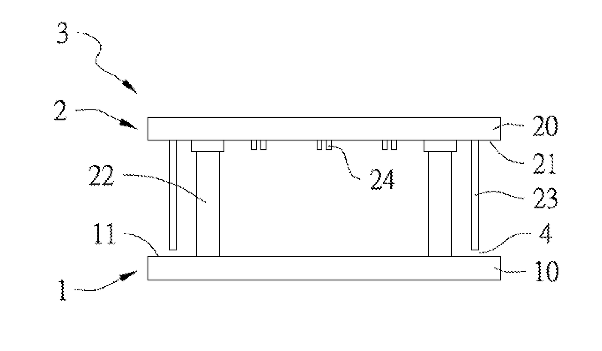
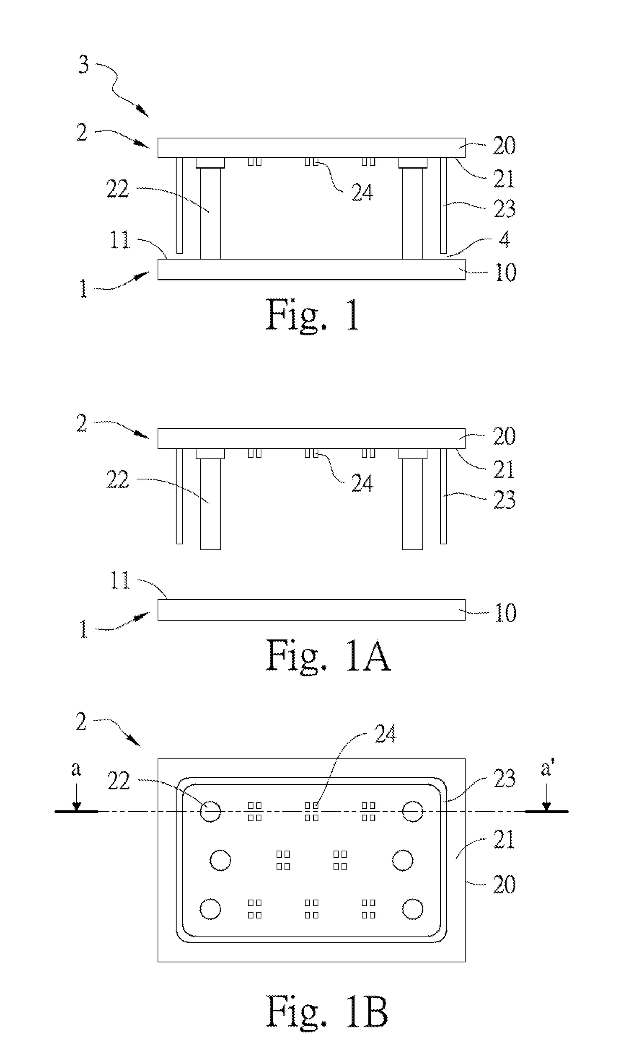
[0049]Please refer to FIG. 1˜FIG. 1B, which are respectively the sectional view and the exploded sectional view and top view before chips stacked of an embodiment of a chip stack having a protection structure for semiconductor device package of the present invention. A chip stack 3 comprises a first chip 1 and a second chip 2, wherein the first chip 1 includes a first substrate 10 and a first surface 11; the second chip 2 includes a second substrate 20, a second surface 21, at least one metal pillar 22, a protection ring 23 and at least one electrical device 24. The first surface 11 of the first chip 1 and the second surface 21 of the second chip 2 are facing to each other. The material of the substrate 10 of the first chip 1 is one material selected from the group consisting of glass, LiTaO3, LiNbO3, quartz, Si, GaAs, GaP, sapphire, Al2O3, InP, SiC, diamond, GaN and AlN. The material of the substrate 20 of the second chip 2 is one material selected from the group consisting of glas...


PUM


Abstract

A chip stack having a protection structure for semiconductor device package comprises a first chip and a second chip stacked with each other. A first surface of the first chip and a second surface of the second chip are facing to each other. At least one metal pillar is formed on at least one of the first surface and the second surface and connected with the other. At least one protection ring is formed on at least one of the first surface and the second surface and having a first gap with the other. At least one electrical device is formed on at least one of the first surface and the second surface and is located inside at least one of the at least one protection ring, wherein the at least one electrical device includes a temperature sensor.

Description

CROSS-REFERENCE TO RELATED DOCUMENTS[0001]The present invention is a continuation in part (CIP) to U.S. patent application Ser. No. 15 / 147,401 entitled “PROTECTION STRUCTURE FOR SEMICONDUCTOR DEVICE PACKAGE” filed on May 5, 2016.FIELD OF THE INVENTION[0002]The present invention relates to a chip stack having a protection structure for semiconductor device package, especially a chip stack having high structure strength and a protection structure for semiconductor device package.BACKGROUND OF THE INVENTION[0003]When a system in package (SIP) includes the surface acoustic wave device or the bulk acoustic wave device etc., during packaging, if the packaging material directly covers the surface acoustic wave device or the bulk acoustic wave device, it will negatively impact the performance of the surface acoustic wave device or the bulk acoustic wave device. Furthermore, when a system in package (SIP) includes the micro-electro-mechanical device or the gyroscope etc., during packaging, i...

Claims


Application Information

Patent Timeline
Patent Type & Authority Applications(United States)
IPC IPC(8): B81B7/00H03H9/25
CPCB81B7/0074H03H9/25B81B2201/0242B81B2201/0278B81B2203/0315B81B2207/11H01L23/562H01L24/29H01L25/162H01L25/165H01L2224/29144H01L2224/29147B81B7/0077G01C19/5783B81B2201/0271H03H9/1014H03H9/1057H03H9/1064H01L2225/06541
Inventor LIAO, PEI-CHUNTING, PO-WEICHIANG, CHIH-FENGWU, YU-KAICHANG, YU-FANLIN, RE-CHINGTSAI, SHU-HSIAOLIN, CHENG-KUO
Owner WIN SEMICON
Why Eureka
Try Eureka