
Semiconductor device and memory device

a memory device and semiconductor technology, applied in semiconductor devices, semiconductor/solid-state device details, electrical apparatus, etc., can solve problems such as data loss, and achieve the effects of reducing the size of transistors, reducing the distance between adjacent memory cells, and improving accuracy

Active Publication Date: 2017-07-27
SEMICON ENERGY LAB CO LTD
View PDF5 Cites 16 Cited by
  • Summary
  • Abstract
  • Description
  • Claims
  • Application Information

AI Technical Summary

Benefits of technology

The present invention relates to a memory device with large storage capacity and low power consumption. The patent describes methods for manufacturing small elements in the memory cells and the need for higher accuracy in patterning. The invention aims to provide a memory device that can store more data and rely on less power than existing devices. The invention can be used in electronic devices that require a large amount of memory.

Problems solved by technology

Although element isolation of transistors is performed using pn junction of silicon in Patent Documents 1 to 5, a leakage current might flow between transistors because of a leakage current flowing in a region of the pn junction, that is, there is a possibility of data loss due to the leakage current.

Method used


Image

  • Semiconductor device and memory device
  • Semiconductor device and memory device
  • Semiconductor device and memory device

Examples


embodiment 1

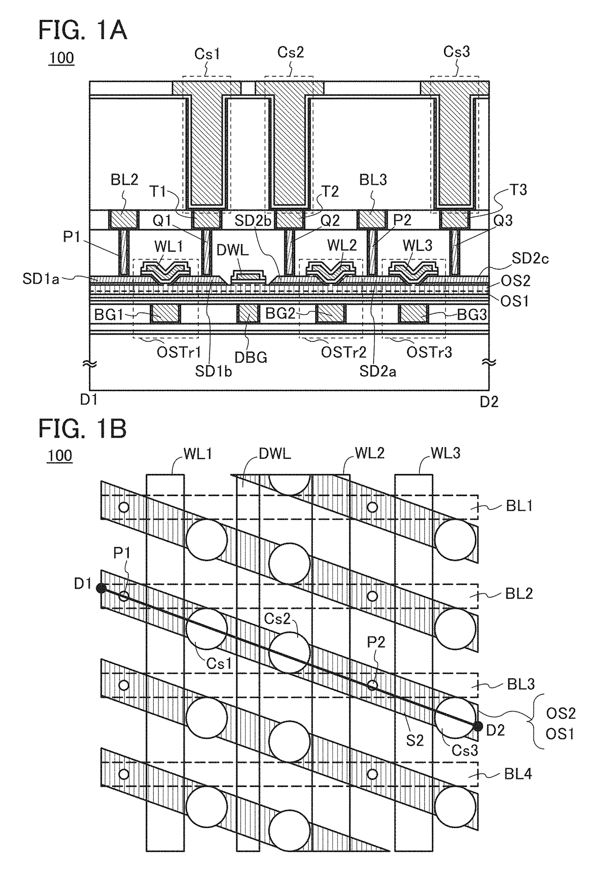
[0063]In this embodiment, an example of a semiconductor device of one embodiment of the present invention will be described.

[0064]FIG. 3A illustrates a circuit configuration example of a memory cell for a DRAM. The details of this circuit configuration will be described in Embodiment 2. The memory cell for a DRAM includes one transistor and one capacitor.

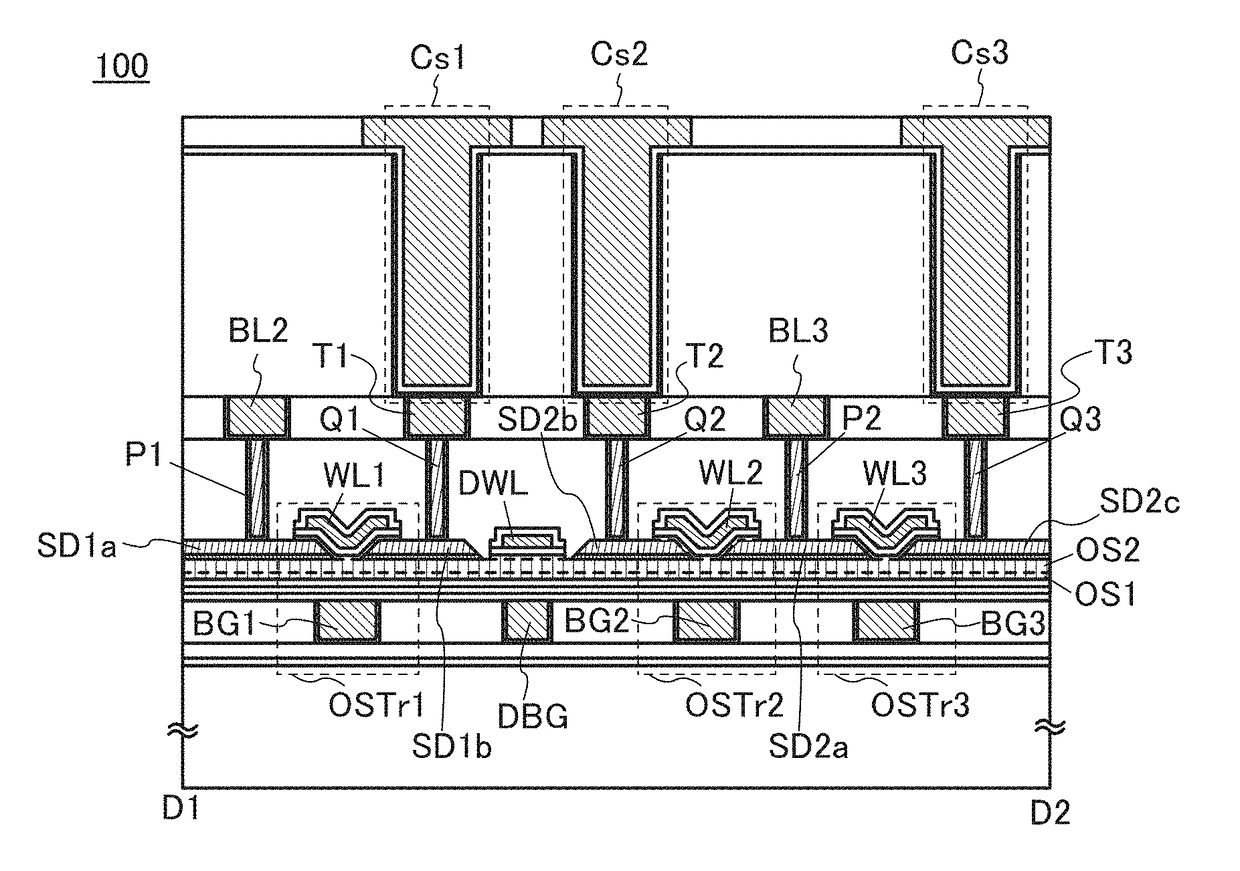
[0065]Next described is a configuration in which a plurality of memory cells each corresponding to the memory cell in FIG. 3A is arranged. A semiconductor device 100 illustrated in FIGS. 1A and 1B has the configuration in which the plurality of memory cells in FIG. 3A is arranged. FIG. 1A is a cross-sectional view of the semiconductor device 100, and FIG. 1B is a top view of the semiconductor device 100. Note that the cross-sectional view of FIG. 1A is taken along a black bold line D1-D2 in the top view of FIG. 1B.

[0066]In the cross-sectional view of the semiconductor device 100 in FIG. 1A, a transistor OSTr1, a transistor OSTr2, a ...

embodiment 2

[0179]In this embodiment, memory cells that can be used in the semiconductor device 100 described in Embodiment 1 are described.

[0180]FIG. 3A illustrates a circuit configuration example of a memory cell for a DRAM. A memory cell 110 includes a transistor MO1 and a capacitor C1. The transistor MO1 is a dual-gate transistor and includes a front gate (simply referred to as gate in some cases) and a back gate.

[0181]A first terminal of the transistor MO1 is electrically connected to a first terminal of the capacitor C1. A second terminal of the transistor MO1 is electrically connected to a wiring BL. A gate of the transistor MO1 is electrically connected to a wiring WL. A back gate of the transistor MO1 is electrically connected to a wiring BGL. A second terminal of the capacitor C1 is electrically connected to a wiring CL.

[0182]The wiring BL functions as a bit line, and the wiring WL functions as a word line. The wiring CL functions as a wiring for applying a predetermined potential to ...

embodiment 3

[0218]A configuration example of a memory device of one embodiment of the present invention will be described with reference to FIG. 12.

[0219]FIG. 12 shows one example of a structure of a memory device. A memory device 2600 includes a peripheral circuit 2601 and a memory cell array 2610. The peripheral circuit 2601 includes a row decoder 2621, a word line driver circuit 2622, a bit line driver circuit 2630, an output circuit 2640, and a control logic circuit 2660.

[0220]The bit line driver circuit 2630 includes a column decoder 2631, a precharge circuit 2632, a sense amplifier 2633, and a write circuit 2634. The precharge circuit 2632 has a function of precharing the wiring BL (not shown in FIG. 12) described in Embodiment 1 and Embodiment 2. The sense amplifier 2633 has a function of amplifying a data signal read from the wiring BL. The amplified data signal is outputt as a digital data signal RDATA to the outside of the memory device 2600 through the output circuit 2640.

[0221]As po...


PUM


Abstract

To provide a semiconductor device with large storage capacity and low power consumption. The semiconductor device includes an oxide semiconductor, a first transistor, a second transistor, and a dummy word line. A channel formation region in the first transistor and a channel formation region in the second transistor are formed in different regions in the oxide semiconductor. The dummy word line is provided to extend between the channel formation region in the first transistor and the channel formation region in the second transistor. By applying a predetermined potential to the dummy word line, the first transistor and the second transistor are electrically isolated in a region of the oxide semiconductor which intersects the dummy word line.

Description

BACKGROUND OF THE INVENTION[0001]1. Field of the Invention[0002]One embodiment of the present invention relates to a semiconductor device and a memory device.[0003]Note that one embodiment of the present invention is not limited to the above technical field. The technical field of the invention disclosed in this specification and the like relates to an object, a method, or a manufacturing method. In addition, one embodiment of the present invention relates to a process, a machine, manufacture, or a composition of matter. Specifically, examples of the technical field of one embodiment of the present invention disclosed in this specification include a semiconductor device, a display device, a liquid crystal display device, a light-emitting device, a power storage device, an imaging device, a memory device, a processor, an electronic device, a method for driving any of them, a method for manufacturing any of them, a method for testing any of them, and a system including any of them.[00...

Claims


Application Information

Patent Timeline
Patent Type & Authority Applications(United States)
IPC IPC(8): H01L27/108H01L27/11H01L29/786H01L23/528H01L27/13H10N97/00
CPCH01L27/10802H01L23/528H01L27/13H01L27/1108H01L29/78648H01L27/10814H01L29/7869H01L28/00H10B43/27H10B12/20H10B10/125H10B12/315
Inventor GODO, HIROMICHIINOUE, TATSUNORI
Owner SEMICON ENERGY LAB CO LTD
Learn More