Group iii nitride semiconductor light-emitting device

a semiconductor and light-emitting device technology, applied in semiconductor devices, basic electric elements, electrical appliances, etc., can solve the problems of difficult capture of carriers by a plurality of pits, difficult to capture carriers, etc., to achieve superior emission efficiency, non-radiative recombination is further suppressed, and the surface flatness of the semiconductor layer is improved.

Active Publication Date: 2017-07-27
TOYODA GOSEI CO LTD
View PDF5 Cites 4 Cited by
  • Summary
  • Abstract
  • Description
  • Claims
  • Application Information

AI Technical Summary

Benefits of technology

[0012]A fourth aspect of the present invention is directed to a specific embodiment of the Group III nitride semiconductor light-emitting device, wherein the n-type semiconductor layer includes a semiconductor layer comprising an n-type GaN layer, a first n-type AlGaN layer, an n-type AlInGaN layer, an ud-AlInGaN layer, an ud-InGaN layer, an ud-GaN layer, and an n-type GaN layer formed in this order on the side far from the light-emitting layer. A potential barrier is formed by the In-doped of the n-type AlInGaN layer. Therefore, the existence probability of electrons and holes is low in the vicinity of threading dislocation. Non-radiative recombination is further suppressed in the threading dislocation. Moreover, the surface flatness of the semiconductor layer is improved by the surfactant effect of In atoms. Thereby, the semiconductor light-emitting device exhibiting superior emission efficiency is achieved.
[0013]A fifth aspect of the present invention is directed to a specific embodiment of the Group III nitride semiconductor light-emitting device, wherein the n-type semiconductor layer includes a semiconductor layer comprising an n-type GaN layer, a first n-type AlGaN layer, an n-type AlInGaN layer, an n-type InGaN layer, an ud-InGaN layer, an ud-GaN layer, and an n-type GaN layer formed in this order on the side far from the light-emitting layer. A potential barrier is formed by the In-doped of the n-type AlInGaN layer. Therefore, the existence probability of electrons and holes is low in the vicinity of threading dislocation. Non-radiative recombination is further suppressed in the threading dislocation. Moreover, the surface flatness of the semiconductor layer is improved by the surfactant effect of In atoms, thereby achieving the semiconductor light-emitting device exhibiting superior emission efficiency.

Problems solved by technology

Therefore, carriers are difficult to be captured by a plurality of pits, that is, carriers are difficult to be captured by threading dislocation being a defect.

Method used


Image

  • Group iii nitride semiconductor light-emitting device
  • Group iii nitride semiconductor light-emitting device
  • Group iii nitride semiconductor light-emitting device

Examples


first embodiment

1. Semiconductor Light-Emitting Device

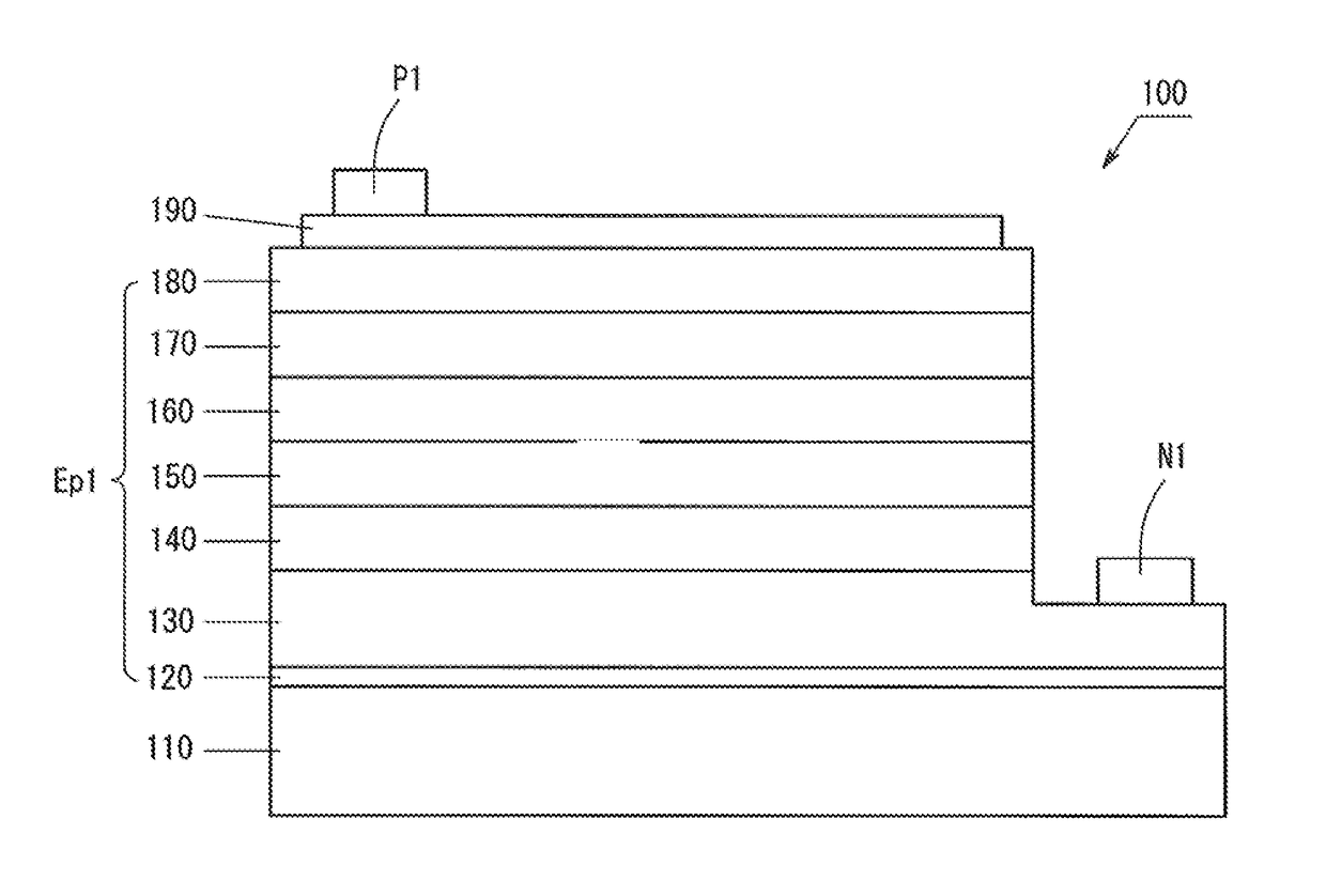
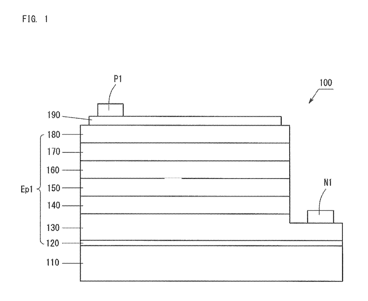
[0034]FIG. 1 is a sketch showing the structure of a light-emitting device 100 according to an embodiment. FIG. 2 is a sketch showing the layered structure of semiconductor layers in the light-emitting device 100. The light-emitting device 100 is a face-up type semiconductor light-emitting device. The light-emitting device 100 has a plurality of Group III nitride semiconductor layers.

[0035]As shown in FIG. 1, the light-emitting device 100 comprises a substrate 110, a low-temperature buffer layer 120, an n-type contact layer 130, an n-side electrostatic breakdown preventing layer 140, an n-side superlattice layer 150, a light-emitting layer 160, a p-type cladding layer 170, a p-type contact layer 180, a transparent electrode 190, an n-electrode N1, and a p-electrode P1. The low-temperature buffer layer 120, the n-type contact layer 130, the n-side electrostatic breakdown preventing layer 140, the n-side superlattice layer 150, the light-emitting l...

second embodiment

[0090]The second embodiment will be described below. The deposition structure of the n-side electrostatic breakdown preventing layer is different between the second embodiment and the first embodiment. Therefore, only differences will be described.

1. N-Side Electrostatic Breakdown Preventing Layer

[0091]As shown in FIG. 13, the light-emitting device 200 of the second embodiment has an n-side electrostatic breakdown preventing layer 240 on the n-type contact layer 130. The n-side electrostatic breakdown preventing layer 240 comprises an n-type GaN layer 241, an n-type AlGaN layer 242, an n-type AlInGaN layer 243, an ud-AlInGaN layer 244, an ud-InGaN layer 245, an ud-GaN layer 246, and an n-type GaN layer 247. That is, the n-type GaN layer 241, the n-type AlGaN layer 242, the n-type AlInGaN layer 243, the ud-AlInGaN layer 244, the ud-InGaN layer 245, the ud-GaN layer 246, and the n-type GaN layer 247 are formed in order on the side far from the light-emitting layer 160.

[0092]The light-...

third embodiment

[0095]The third embodiment will be described below. The deposition structure of the n-side electrostatic breakdown preventing layer is different between the third embodiment and the first embodiment. Therefore, only differences will be described.

1. N-Side Electrostatic Breakdown Preventing Layer

[0096]As shown in FIG. 14, the light-emitting device 300 of the third embodiment has an n-side electrostatic breakdown preventing layer 340 on the n-type contact layer 130. The n-side electrostatic breakdown preventing layer 340 comprises an n-type GaN layer 341, an n-type AlGaN layer 342, an n-type AlInGaN layer 343, an n-type InGaN layer 344, an ud-InGaN layer 345, an ud-GaN layer 346, and an n-type GaN layer 347. That is, the n-type GaN layer 341, the n-type AlGaN layer 342, the n-type AlInGaN layer 343, the n-type InGaN layer 344, the ud-InGaN layer 345, the ud-GaN layer 346, and the n-type GaN layer 347 are formed in order on the side far from the light-emitting layer 160.

[0097]The light...


PUM


Abstract

The present invention provides a Group III nitride semiconductor light-emitting device in which electrons and holes are suppressed from being captured by threading dislocation, and a production method therefor. The light-emitting device comprises an n-type contact layer, an n-side electrostatic breakdown preventing layer, an n-side superlattice layer, a light-emitting layer, a p-type cladding layer, a p-type contact layer, a transparent electrode, an n-electrode, and a p-electrode. The light-emitting device has a plurality of pits extending from the n-type semiconductor layer to the p-type semiconductor layer. The n-side electrostatic breakdown preventing layer has an n-type AlGaN layer. The n-type AlGaN layer includes starting points of the pits.

Description

BACKGROUND OF THE INVENTION[0001]Field of the Invention[0002]The present invention relates to a Group III nitride semiconductor light-emitting device and a production method therefor, more specifically, to a method for producing a Group III nitride semiconductor light-emitting device having pits.[0003]Background Art[0004]A Group III nitride semiconductor light-emitting device comprises a light-emitting layer which emits light through recombination of electrons and holes, an n-type semiconductor layer, and a p-type semiconductor layer. When producing the Group III nitride semiconductor light-emitting device, a semiconductor layer is epitaxially grown on a substrate. In this case, threading dislocation occurs in the semiconductor layer due to lattice mismatch between the substrate and the semiconductor layer. In the threading dislocation, non-radiative recombination of electrons and holes occurs. Non-radiative recombination refers to a recombination of electrons and holes which genera...

Claims


Application Information

Patent Timeline
Patent Type & Authority Applications(United States)
IPC IPC(8): H01L33/00H01L33/06H01L33/22H01L33/32H01L33/24
CPCH01L33/0025H01L33/32H01L33/06H01L33/22H01L33/24H01L33/20
Inventor NAGATA, KENGO
Owner TOYODA GOSEI CO LTD
Why Eureka
Try Eureka