
Organic el display panel, display device incorporating same, and organic el display panel manufacturing method

a technology of organic el and display panels, which is applied in the direction of organic semiconductor devices, thermoelectric devices, solid-state devices, etc., can solve the problems of increasing manufacturing costs, increasing longevity, and increasing manufacturing costs, so as to reduce the current required to obtain the desired luminance, increase the lifespan of current-driven organic el elements, and improve manufacturing costs and productivity

Active Publication Date: 2017-08-03
JOLED INC
View PDF0 Cites 20 Cited by
  • Summary
  • Abstract
  • Description
  • Claims
  • Application Information

AI Technical Summary

Benefits of technology

The present patent relates to an organic EL display panel with improved charge generating layer formation and optical length ranges for efficient light extraction. These ranges ensure that blue light emitted from both layers is efficiently extracted, while suppressing unwanted blue light from other layers. This results in a decrease in the current required for a desired luminance and increased lifespan of current-driven organic EL elements. Additionally, the optical lengths in the red and green sub-pixels improve the light extraction efficiency of red and green light, while suppressing unwanted blue light. The optical lengths also bring the color of a mix of light closer to white light. Overall, the technical effects of the patent are improved manufacturing cost and productivity, increased lifespan, and improved color purity.

Problems solved by technology

Among red, green, and blue colors of organic EL elements, lifespan of blue organic EL elements tends to be shortest, and therefore increasing longevity of blue organic EL elements is a technical problem for increasing longevity of display devices.
In such a case, material that forms light-emitting layers or functional layers attaches to portions of the shadow mask other than the openings, and this loss of material is a cause of increased manufacturing cost.
Further, accurate alignment of openings of the precision shadow mask to sub-pixels is a factor lowering production efficiency, and in particular when producing large organic EL display panels the alignment of shadow mask to sub-pixels is very difficult.
However, there is a problem in that an organic EL element formed by using a wet process has a shorter lifespan that an organic EL element formed by using vacuum deposition.

Method used


Image

  • Organic el display panel, display device incorporating same, and organic el display panel manufacturing method
  • Organic el display panel, display device incorporating same, and organic el display panel manufacturing method
  • Organic el display panel, display device incorporating same, and organic el display panel manufacturing method

Examples


embodiment 1

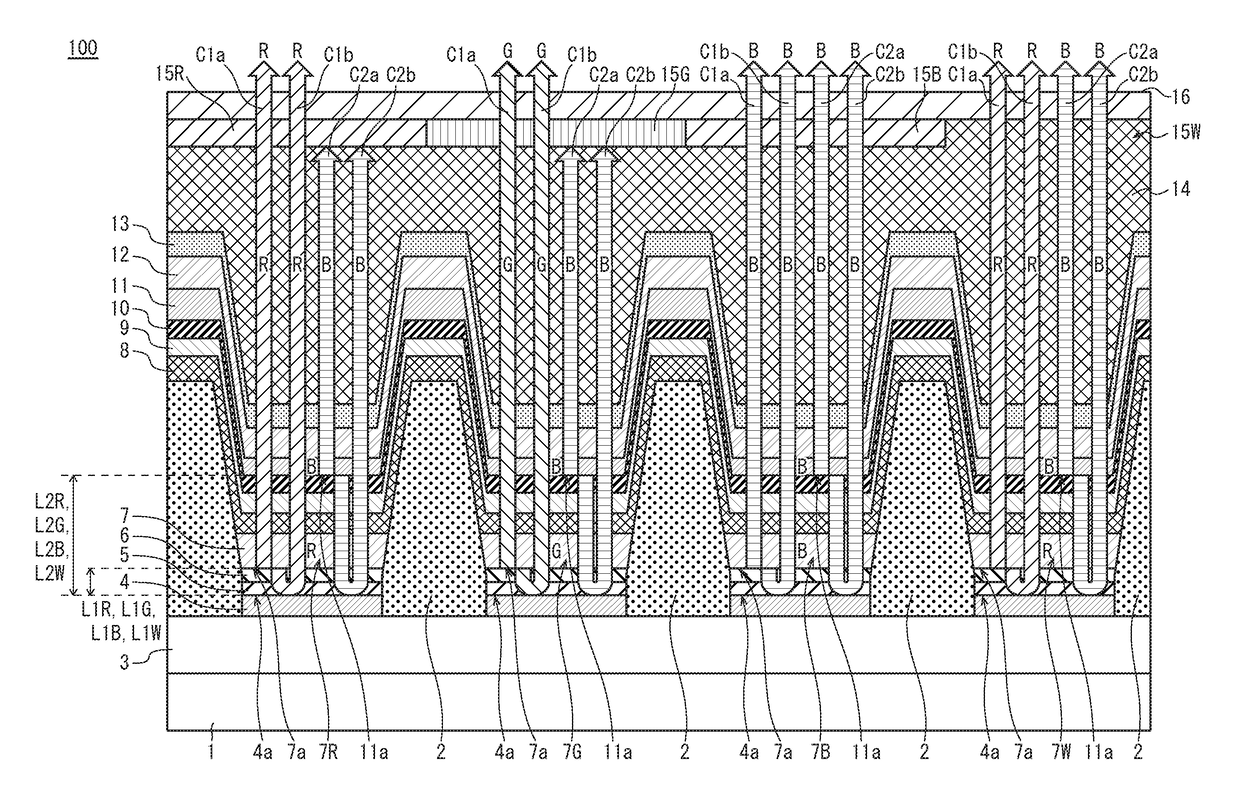
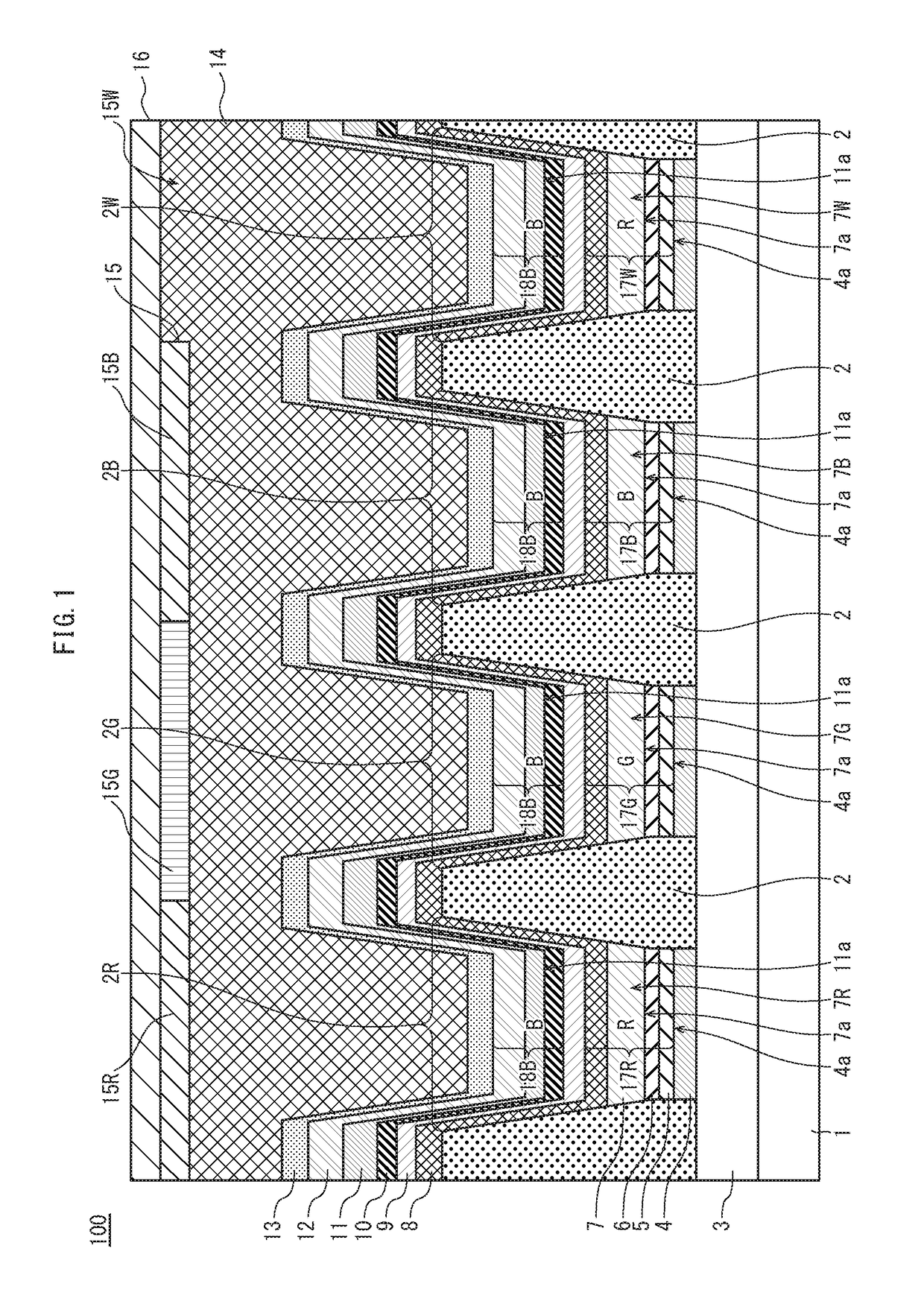
[0169]The organic EL display panel 200 includes the second substrate 16, the color filter 15, the banks 2, the insulating layer 3, light-transmissive electrodes 213, the first hole injection layers 5, the first hole transport layers 6, the first red light-emitting layer 7R, the green light-emitting layer 7G, the first blue light-emitting layer 7B, the second red light-emitting layer 7W, the first electron transport layer 8, the charge generating layer 9, the second hole transport layer 10, the second blue light-emitting layer 11, the second electron transport layer 12, a light-reflective electrode 204, the protective layer 14, and the second substrate 1. The functions of each layer, materials, and method of manufacture are the same as for Embodiment 1, and therefore description thereof is not repeated here.

[9. Optical Design (Bottom-Emission)]

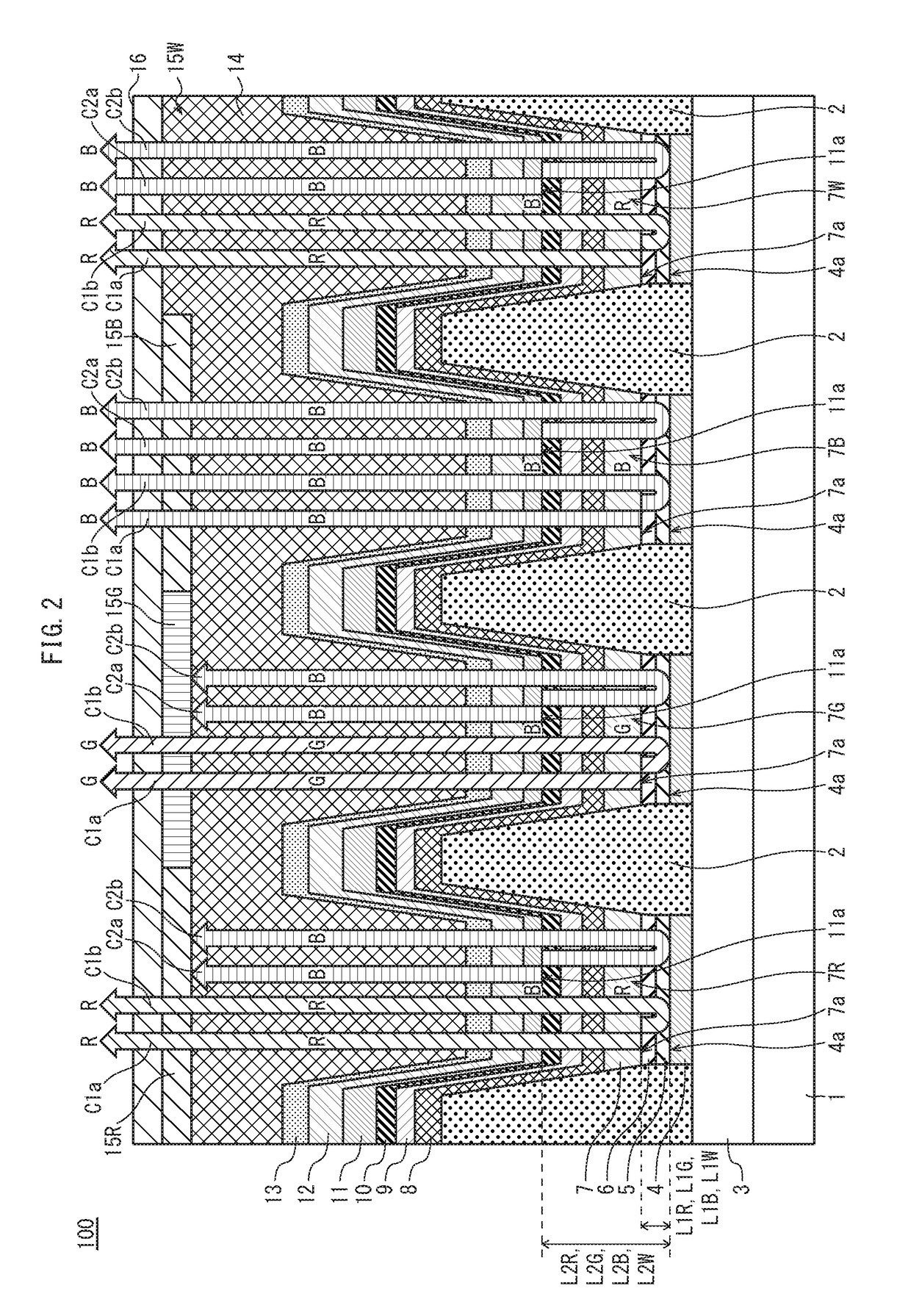
[0170]FIG. 10 illustrates optical paths of light emitted from the organic EL elements in sub-pixel regions.

[0171]An optical path C1a is an opt...


PUM


Abstract

An organic EL display panel includes light-reflective electrodes, a first red light-emitting layer, a green light-emitting layer, a first blue light-emitting layer, a second red light-emitting layer, a charge generating layer, a second blue light-emitting layer, and a light-transmissive electrode. In a red and a white sub-pixel region, a first optical length is from 20 nm to 50 nm, and a second optical length is from 210 nm to 230 nm. In a green sub-pixel region, the first optical length is from 20 nm to 50 nm, and the second optical length is from 240 nm to 295 nm. In a blue sub-pixel region, the first optical length is from 20 nm to 60 nm, and the second optical length is from 195 nm to 205 nm.

Description

TECHNICAL FIELD[0001]The present disclosure relates to organic electroluminescence (EL) display panels incorporating tandem-structure organic EL elements, display devices incorporating organic EL display panels, and organic EL display panel manufacturing methods.BACKGROUND ART[0002]In recent years, as display panels used in display devices such as digital televisions, organic electroluminescence (EL) display panels that use electroluminescence of organic materials are being implemented in which a plurality of organic EL elements are arrayed on a substrate.[0003]As an organic EL display panel configuration, typically thin film transistor (TFT) drive circuitry is disposed on a substrate, an insulating layer is disposed on the TFT drive circuitry, and a plurality of organic EL elements are arrayed thereon. An organic EL element has, at minimum, a light-emitting layer sandwiched between a pair of electrodes (anode and cathode). Typically, an organic EL element has a hole injection layer...

Claims


Application Information

Patent Timeline
Patent Type & Authority Applications(United States)
IPC IPC(8): H01L51/50H01L51/52H01L51/56H01L27/32
CPCH01L51/5044H01L27/3246H01L27/3213H01L2251/5315H01L51/5218H01L51/5234H01L51/56H01L27/322H10K59/351H10K50/131H10K59/876H10K59/80524H10K50/818H10K50/828H10K59/38H10K59/122H10K71/00H10K50/852H10K2102/3026
Inventor MATSUSUE, NORIYUKIYONEDA, KAZUHIROHOANG, MINH HIEP
Owner JOLED INC
Learn More