Liquid crystal display device

a liquid crystal display and display screen technology, applied in semiconductor devices, optics, instruments, etc., can solve the problems of lowering display quality, reducing the area of each pixel, and reducing the distance between the contact hole in one pixel and the contact hole in the other pixel, so as to improve the screen resolution of lcds, especially small ones, the effect of enhancing resolution

Active Publication Date: 2017-08-17
JAPAN DISPLAY INC
View PDF12 Cites 9 Cited by
  • Summary
  • Abstract
  • Description
  • Claims
  • Application Information

AI Technical Summary

Benefits of technology

[0009]The screen resolution of LCDs, especially small ones, is being enhanced. Enhancing resolution requires the area of each pixel to be reduced. This means that within a pixel, the area of the contact hole that is used to connect the pixel electrode to the source electrode of the TFT occupies a larger portion of that pixel. Moreover, the distance between the contact hole in a pixel and the contact hole in another pixel is reduced as well.
[0010]In LCDs, an alignment film is formed to perform initial alignment on the liquid crystal molecules. The material of the alignment film is in the form of liquid at the time of application and baked to form the alignment film. As a contact hole becomes smaller, the material of the alignment film is more likely to be repelled and less likely to be formed in the contact hole. When the material of the alignment film does not flow into the contact hole, the thickness of the alignment film formed around the contact hole does not become uniform. In other words, at the edge of the alignment film that results from the material of the alignment film not flowing into the contact hole, the amount of the alignment film increases by the material of the amount that should have flowed into the contact hole. Also, due to the surface energy at the edge, the alignment film is formed thicker near the contact hole. If such a region where the alignment film has been formed thick passes a masked area and reaches a transmissive area, the voltage applied to the liquid crystal layer may decrease in that transmissive area, or the gaps in the liquid crystal layer at the transmissive area may be smaller than in other areas. Thus, the display quality in the transmissive area may be reduced (dim-colored spots) relative to other regions.
[0014]An object of the present invention is thus to prevent the phenomenon of the alignment film not being formed in contact holes and reduce display unevenness resulting from light leakage.Means for Solving the Problems

Problems solved by technology

When the material of the alignment film does not flow into the contact hole, the thickness of the alignment film formed around the contact hole does not become uniform.
However, as stated above, if regions where the alignment film has nonuniform thicknesses reach a transmissive area (i.e., area not masked by a black matrix), this does pose a problem.
In such a case, the regions where the alignment film is not formed reach a display area, thus lowering display quality.
Therefore, high-resolution LCDs are prone to the non-uniformity of alignment film thickness and enlarged regions where the alignment film is not formed, for the pixel pitch is small in such LCDs.
Regions where the thickness of the alignment film is not uniform are present in multiple pixels, and those regions cause display unevenness.

Method used


Image

  • Liquid crystal display device
  • Liquid crystal display device
  • Liquid crystal display device

Examples


Embodiment Construction

[0036]Embodiments of the present invention will now be described in detail.

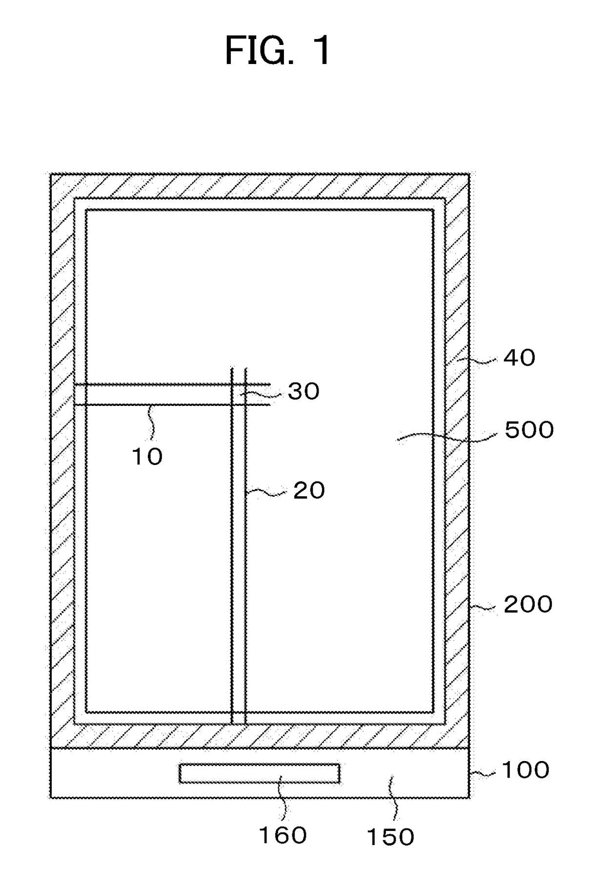
[0037]FIG. 1 is a plan view of an LCD to which the invention is applied. In FIG. 1, a TFT substrate 100 and a counter substrate 200 are glued by a sealing material 40, and a liquid crystal layer is sandwiched between the TFT substrate 100 and the counter substrate 200. The TFT substrate 100 is formed larger than the counter substrate 200, and the section of the TFT substrate 100 that does not overlap any other layer serves as a terminal section 150. Formed at the terminal section 150 are an IC driver 160 for driving an LCD panel and terminals to which to connect a flexible printed circuit board for supplying to the LCD panel electric power, video signals, clock signals, and so on.

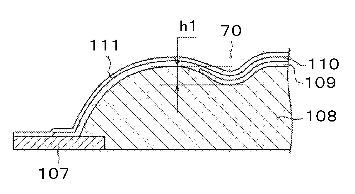
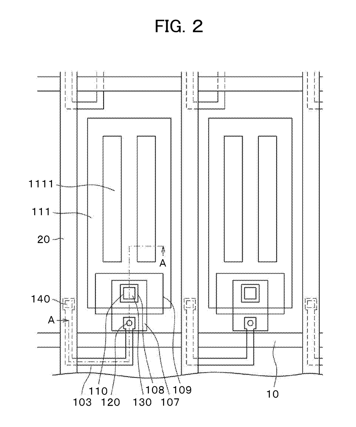
[0038]As illustrated in FIG. 1, within a display area 500, gate lines 10 extend in a first direction and are arranged in a second direction. Also, video signal lines 20 extend in the second direction and are arranged in the first dir...


PUM

PropertyMeasurementUnit
heightaaaaaaaaaa
thickaaaaaaaaaa
thicknessaaaaaaaaaa

Abstract

A liquid crystal display device has pixels in a TFT substrate, each of the pixels has a TFT. An organic insulting film 108 is formed to cover the TFT. A first electrode 109 and a second electrode 111 are formed above the organic insulting film 108 with an inorganic insulating film 110 placed between the first electrode 109 and the second electrode 111. An alignment film is formed on the first electrode 109 and the second electrode 111. The second electrode 111 connects with the TFT through a contact hole formed in the organic insulating film 108. A cross section of the organic insulating film 108 that includes the contact hole and is parallel to the second direction has a convex section and a concave section 70 at a bank located near the contact hole, the convex section being located closer to the contact hole than the concave section 70.

Description

CLAIM OF PRIORITY[0001]The present application claims priority from Japanese Patent Application JP 2016-027833 filed on Feb. 17, 2016, the content of which is hereby incorporated by reference into this application.BACKGROUND OF THE INVENTION[0002]1. Field of the Invention[0003]The present invention relates to display devices and particularly to a high-resolution liquid crystal display device (LCD) that prevents display unevenness that results from the presence of regions where an alignment film is not formed.[0004]2. Description of the Related Art[0005]A typical LCD includes a thin film transistor (TFT) substrate, a counter substrate, and a liquid crystal layer placed between them. On the TFT substrate, pixels each having a pixel electrode, a TFT, and the like are formed in the form of a matrix. Images are produced by controlling the transmittance rate of light passing through the liquid crystal molecules on a pixel-by-pixel basis.[0006]An organic passivation film is formed to cover...

Claims


Application Information

Patent Timeline
Patent Type & Authority Applications(United States)
IPC IPC(8): G02F1/1337G02F1/1368G02F1/1335G02F1/1362G02F1/1333
CPCG02F1/1337G02F1/136227G02F1/133345G02F1/136286G02F2001/133776G02F1/1368H01L27/124H01L27/1248G02F1/133512G02F1/133371G02F1/133357G02F1/134372G02F1/133776
Inventor ISHIKAWA, TOMOKAZUKURAMOTO, YUKIMIYAIRI, HIROSHIKOBAYASHI, RYOTASUGIMOTO, KATSUTO
Owner JAPAN DISPLAY INC
Why Eureka
Try Eureka