

Inspection Apparatus and Method, Lithographic Apparatus, Method of Manufacturing Devices and Computer Program
a technology of lithographic apparatus and lithography, applied in the direction of instruments, photomechanical treatment, optics, etc., can solve the problems of inability to image the dimensions of modern product structures by optical metrology techniques, and the time-consuming of sem
- Summary
- Abstract
- Description
- Claims
- Application Information
AI Technical Summary
Benefits of technology
Problems solved by technology
Method used
Image

Examples
Embodiment Construction
[0026]Before describing embodiments of the invention in detail, it is instructive to present an example environment in which embodiments of the present invention may be implemented.
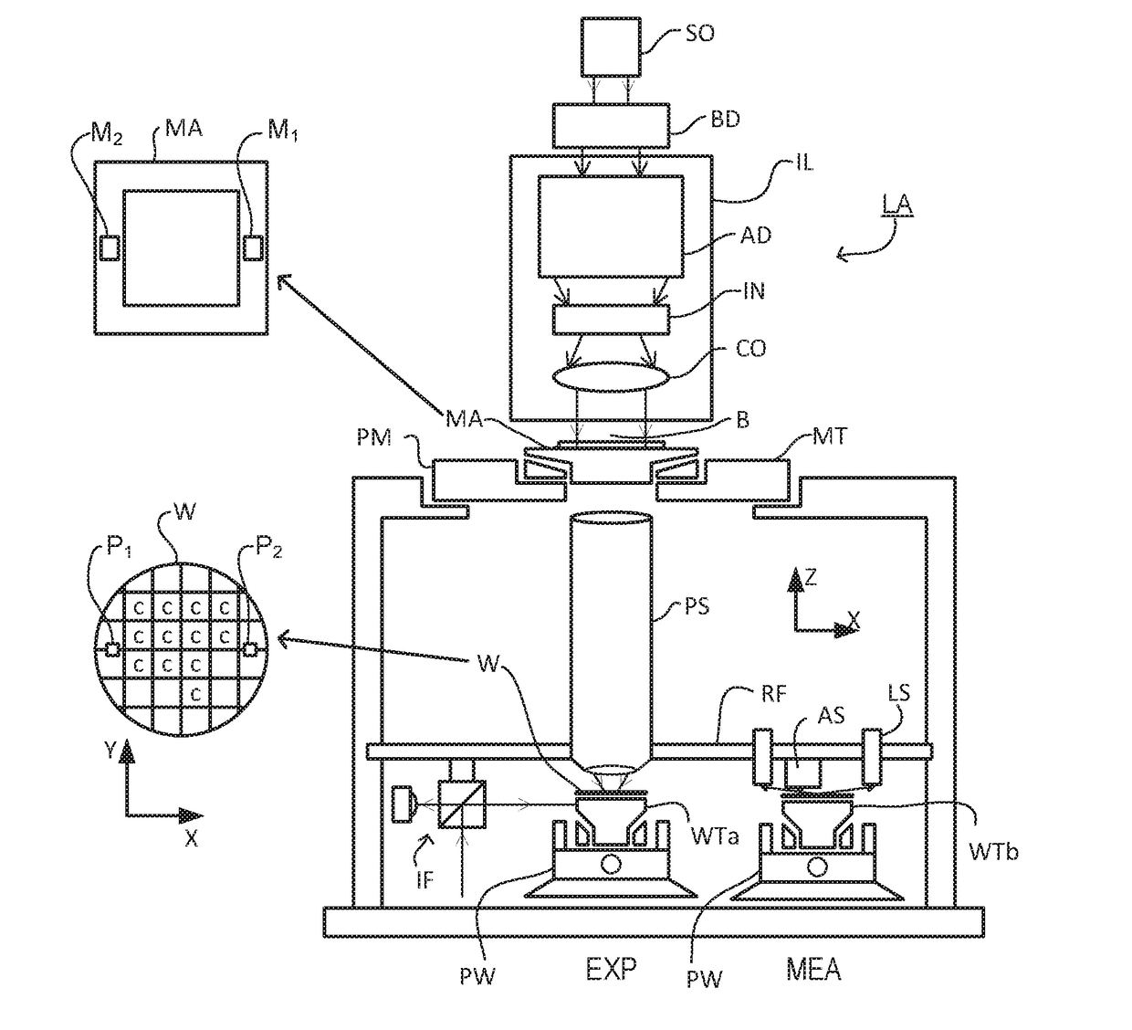
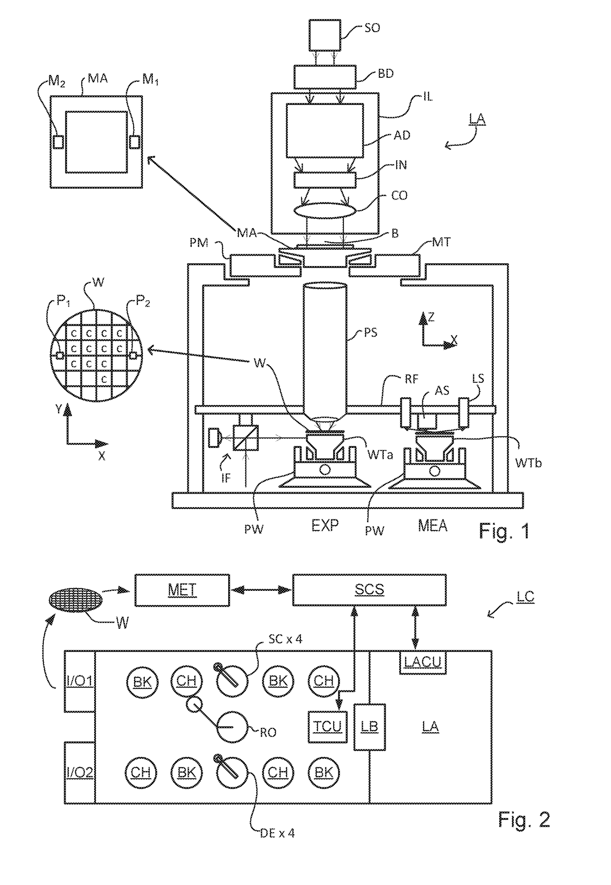
[0027]FIG. 1 schematically depicts a lithographic apparatus LA. The apparatus includes an illumination system (illuminator) IL configured to condition a radiation beam B (e.g., UV radiation or DUV radiation), a patterning device support or support structure (e.g., a mask table) MT constructed to support a patterning device (e.g., a mask) MA and connected to a first positioner PM configured to accurately position the patterning device in accordance with certain parameters; two substrate tables (e.g., a wafer table) WTa and WTb each constructed to hold a substrate (e.g., a resist coated wafer) W and each connected to a second positioner PW configured to accurately position the substrate in accordance with certain parameters; and a projection system (e.g., a refractive projection lens system) PS configured t...
PUM
 Abstract
Description
Claims
Application Information