

Pixel structure and fabrication method thereof
a technology of pixel structure and fabrication method, which is applied in the direction of semiconductor devices, semiconductor/solid-state device details, electrical devices, etc., can solve the problems of display quality reduction, and achieve the effect of avoiding the problem of display quality reduction
- Summary
- Abstract
- Description
- Claims
- Application Information
AI Technical Summary
Benefits of technology
Problems solved by technology
Method used
Image

Examples
Embodiment Construction
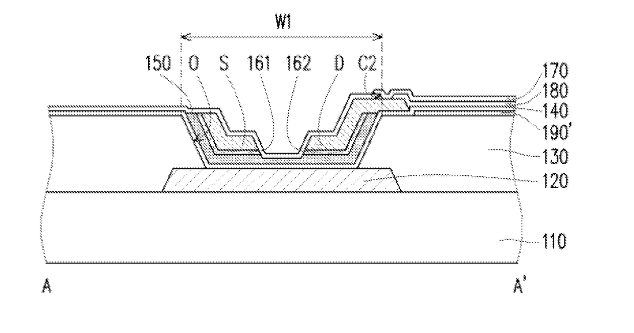
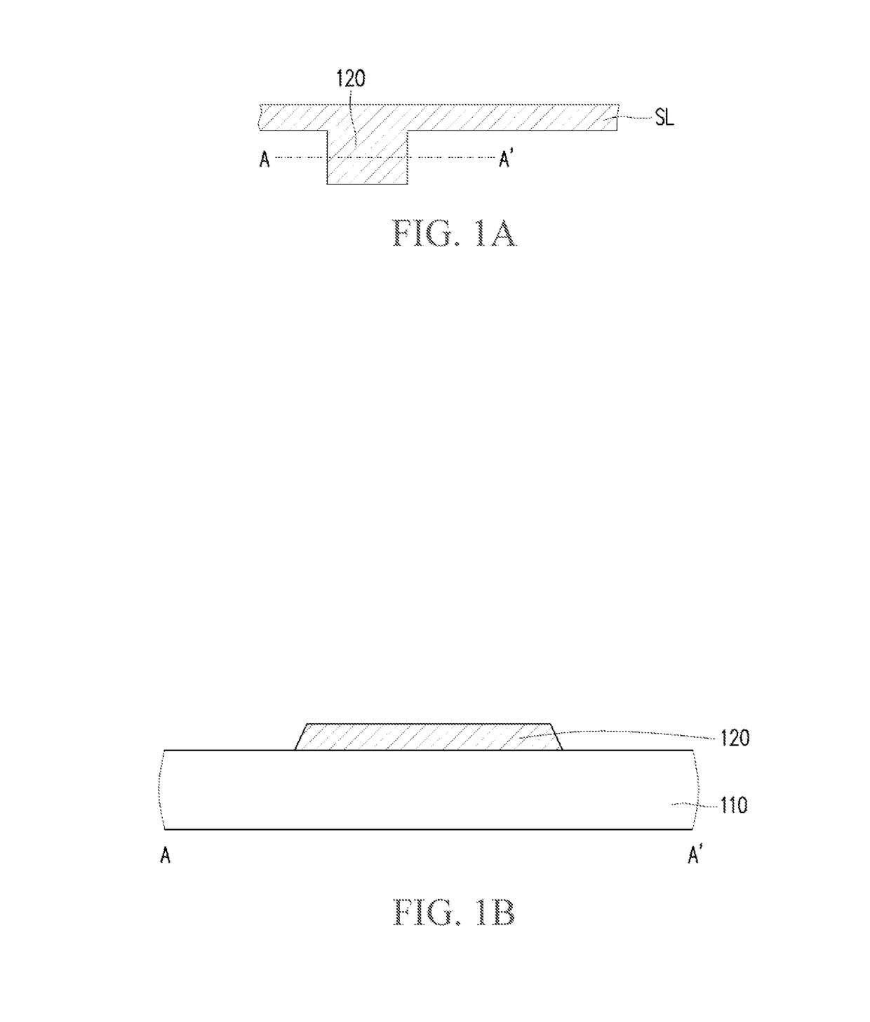
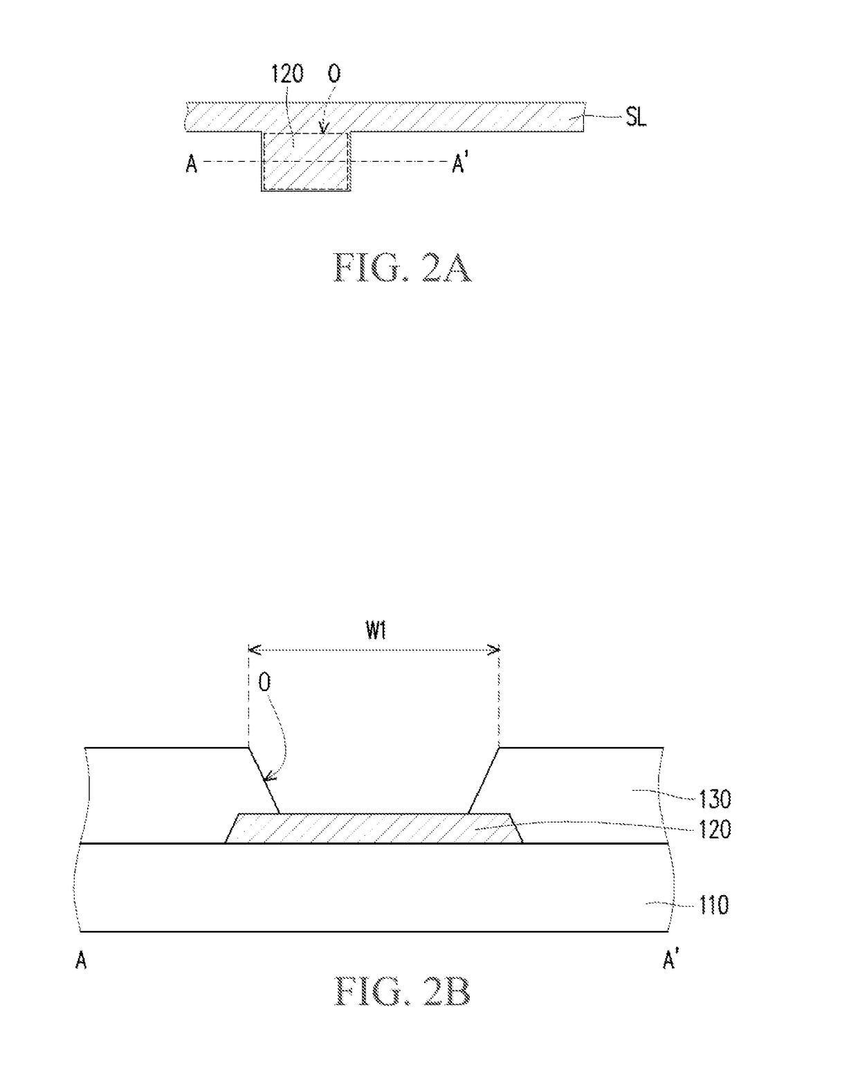
[0022]FIG. 1A to FIG. 6A are top views of a process of a fabrication method for a pixel structure according to an embodiment of the present invention. FIG. 1B, FIG. 2B, FIG. 3B, FIG. 3C, FIG. 4B, FIG. 5B, and FIG. 6B respectively are cross-section diagrams of the process of the fabrication method for a pixel structure in FIG. 1A to FIG. 6A along a section line AA′. Referring to FIG. 1A and FIG. 1B, a substrate 110 is provided. The material of the substrate 110 may be glass, quartz, organic polymer, or opaque / reflective material (for example, conductive material, metal, wafer, ceramics, or other suitable materials), or other suitable materials. A gate electrode 120 and a scan line SL connected to the gate electrode 120 are formed on the substrate 110. In this embodiment, the fabrication method for the gate electrode 120 and the scan line SL includes, for example, depositing a metallic material layer (not shown) and performing a patterning process on the metallic material layer to for...
PUM
 Abstract
Description
Claims
Application Information