Organic Light Emitting Diode Device and Array Substrate

a light-emitting diode and array substrate technology, applied in the field of display technology, can solve the problems of low resistance transparent electrodes, uneven light-emitting, and excessive horizontal resistance, and achieve the effect of reducing the resistance of transparent anodes, and improving the horizontal conductivity of transparent anodes

Inactive Publication Date: 2017-09-14
TCL CHINA STAR OPTOELECTRONICS TECH CO LTD
View PDF3 Cites 4 Cited by
  • Summary
  • Abstract
  • Description
  • Claims
  • Application Information

AI Technical Summary

Benefits of technology

[0016]a metal layer disposed on a surface of the first transparent anode and covering the surface of the first transparent anode for reducing a resistance of the transparent anode of the organic light emitting diode device in a horizontal direction;
[0034]a metal layer disposed on a surface of the first transparent anode and covering the surface of the first transparent anode completely for reducing a resistance of the transparent anode of the organic light emitting diode device in a horizontal direction; and
[0055]a metal layer disposed on a surface of the first transparent anode and covering the surface of the first transparent anode completely for reducing a resistance of the transparent anode of the organic light emitting diode device in a horizontal direction; and
[0063]The embodiment of the present invention provides an organic light emitting diode device and an array substrate. The organic light emitting diode device of the embodiment of the present invention can reduce a resistance of the transparent anode in a horizontal direction through setting two transparent anode layers and disposing a metal layer therebetween, and can further improve a horizontal conductivity of the transparent anode layers, thereby solving the problem of uneven light emission of the organic light emitting diode device due to the greater horizontal resistance of the transparent anode for improving the quality of the screen display.

Problems solved by technology

Currently, during the operation of a large area OLED (organic light emitting diode) display panel, a phenomenon of light emitting unevenly often occurs.
The phenomenon is caused by a variety of reasons, the main reasons being the uneven distribution of vertical resistance and the excessively large amount of horizontal resistance.
Making low resistance transparent electrodes is currently difficult.
During the operation of the organic light emitting diode, when a current is applied to the edge of the transparent anode, it is difficult for the current to reach a central region of the transparent anode.
Therefore, uneven light emitting of the OLED device is caused.

Method used


Image

  • Organic Light Emitting Diode Device and Array Substrate
  • Organic Light Emitting Diode Device and Array Substrate
  • Organic Light Emitting Diode Device and Array Substrate

Examples


embodiment 1

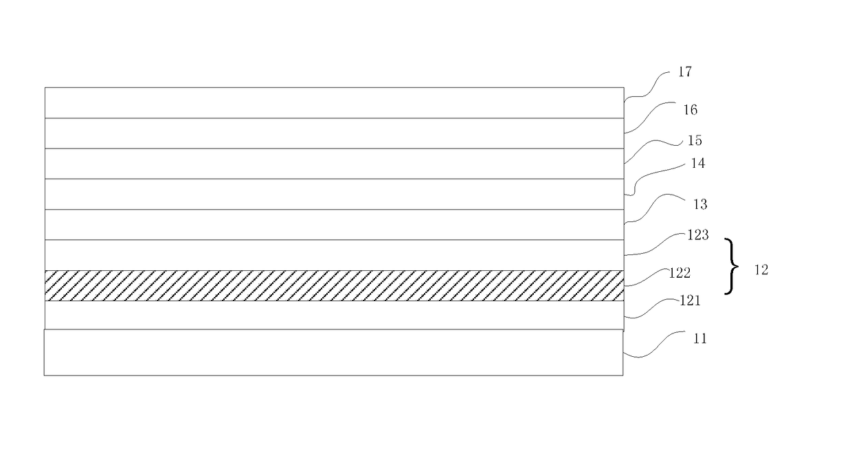
[0070]Referring to FIG. 1, the embodiment of the present invention provides an organic light emitting diode device, comprising:

[0071]a base substrate 11, which is preferably a glass substrate;

[0072]a transparent anode 12 disposed on the base substrate utilized for being driven to output a hole (alternatively referred to as a carrier), for example, when the organic light emitting diode device is in operation, the transparent anode 12 is connected to a positive electrode of a drive voltage and a transparent cathode 17 is connected to a negative electrode of the drive voltage;

[0073]a hole injecting layer 13 disposed on the transparent anode 12 for receiving the hole output by the transparent anode 12;

[0074]a hole transporting layer 14 disposed on the hole injection layer 13 for transporting the hole of the hole injecting layer to an organic light-emitting layer 15, in the embodiment, the hole transporting layer 14 can reduce an interface barrier between the transparent anode 12 and the...

embodiment 2

[0102]This embodiment of the present invention provides an organic light emitting diode array substrate, comprising:

[0103]a base substrate; an organic light emitting diode device disposed on the base substrate; and

[0104]a thin film transistor disposed on the base substrate for controlling light emitting of the corresponding organic light emitting diode device.

[0105]Referring to FIG. 1, the organic light emitting diode device comprises:

[0106]a transparent anode 12 disposed on the base substrate utilized for being driven to output a hole (alternatively referred to as a carrier), for example, when the organic light emitting diode device is in operation, the transparent anode 12 is connected to a positive electrode of a drive voltage and a transparent cathode 17 is connected to a negative electrode of the drive voltage;

[0107]a hole injecting layer 13 disposed on the transparent anode 12 for receiving the hole output by the transparent anode 12;

[0108]a hole transporting layer 14 disposed...


PUM


Abstract

An organic light emitting diode device and array substrate having the organic light emitting diode are provided. The organic light emitting diode device of the embodiment of the present invention can reduce a resistance of the transparent anode, which is used for providing holes, in a horizontal direction through setting two transparent anode layers and disposing a metal layer therebetween, and further can improve a horizontal conductivity of the transparent anode, thereby solving the problem of uneven light emission of the organic light emitting diode device due to the greater horizontal resistance of the transparent anode for improving the quality of the screen display having the array substrate.

Description

FIELD OF THE INVENTION[0001]The present invention relates to display technology, and more particularly to an organic light emitting diode device and array substrate.BACKGROUND OF THE INVENTION[0002]Currently, during the operation of a large area OLED (organic light emitting diode) display panel, a phenomenon of light emitting unevenly often occurs. The phenomenon is caused by a variety of reasons, the main reasons being the uneven distribution of vertical resistance and the excessively large amount of horizontal resistance. Besides, the vertical resistance is mainly determined by an energy level structure, carrier mobility, and a thickness of each layer of the device, and the horizontal resistance is mainly determined by a conductivity of a transparent electrode.[0003]Making low resistance transparent electrodes is currently difficult. Thus, the horizontal resistance of the transparent electrode (i.e., the resistance in the horizontal direction) is relatively high. During the operat...

Claims


Application Information

Patent Timeline
Patent Type & Authority Applications(United States)
IPC IPC(8): H01L51/52H01L51/50H01L27/32
CPCH01L51/5215H01L27/3244H01L51/5212H01L51/5088H01L2251/558H01L51/5012H01L51/5072H01L51/5234H01L51/5056H10K59/00H10K50/00H10K50/81H10K50/814H10K50/816H10K50/11H10K50/15H10K50/16H10K50/17H10K50/828H10K59/12H10K2102/351
Inventor XU, CHAO
Owner TCL CHINA STAR OPTOELECTRONICS TECH CO LTD
Why Eureka
Try Eureka