Semiconductor device and production method therefor

a technology of semiconductors and semiconductors, applied in the direction of semiconductor devices, basic electric elements, electrical equipment, etc., can solve the problems of insufficient improvement of breakdown voltage and inability to reach the design value of breakdown voltage, and achieve the effects of low carrier concentration, small thickness, and easy forming

Active Publication Date: 2017-10-05
TOYODA GOSEI CO LTD
View PDF3 Cites 1 Cited by
  • Summary
  • Abstract
  • Description
  • Claims
  • Application Information

AI Technical Summary

Benefits of technology

[0016]According to the production method of the present invention, the third layer of the electric field relaxation region and the fourth layer of the device region can be simultaneously formed, thereby easily forming the third layer.
[0017]In the present invention, the third layer has a low carrier concentration and a small thickness. Therefore, when a reverse voltage is applied, the third layer is depleted earlier than the second layer. The depleted region serves as a region for relaxing the electric field concentration at the pn interface exposed at the end surfaces of the semiconductor device, thereby remarkably improving the breakdown voltage.

Problems solved by technology

When a reverse voltage is applied to the semiconductor device, there is a problem that the breakdown voltage does not reach the design value because the electric field is concentrated at the pn interface exposed on the terminal surface.
However, breakdown voltage is not sufficiently improved even in the structure of Japanese Patent No. 5691259, further improvement in the breakdown voltage was sought.

Method used


Image

  • Semiconductor device and production method therefor
  • Semiconductor device and production method therefor
  • Semiconductor device and production method therefor

Examples


embodiment 1

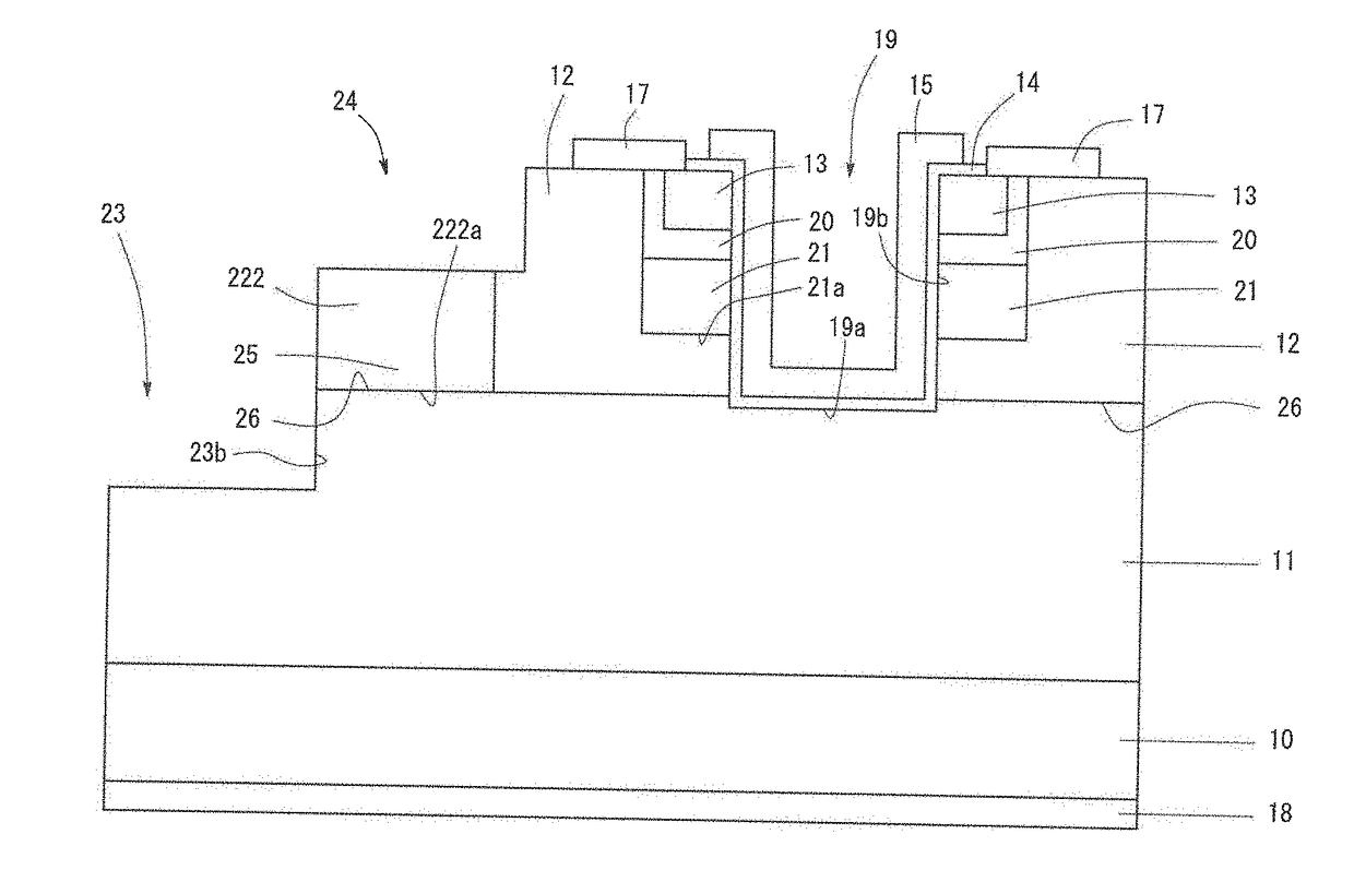
[0032]FIG. 1 is a sketch showing the structure of a semiconductor device according to Embodiment 1. The semiconductor device according to Embodiment 1 is a trench-type vertical MOSFET, and comprises a substrate 10, a first n-type layer 11 (drift region) deposited on the substrate 10, a p-type layer 12 (body region) deposited on the first n-type layer 11, and a second n-type layer 13 (source region) formed on a part of the p-type layer 12 as shown in FIG. 1. The semiconductor device further comprises a gate insulating film 14, a gate electrode 15, a source electrode 17, a drain electrode 18, and a trench 19. The semiconductor device according to Embodiment 1 comprises a device region 1 being disposed at the center of the device and functioning and operating as MOSFET, and a terminal region 2 being formed in the outer periphery of the device region 1 so as to surround the device region 1. The terminal region 2 is a region having a structure to improve the breakdown voltage of the semi...

embodiment 2

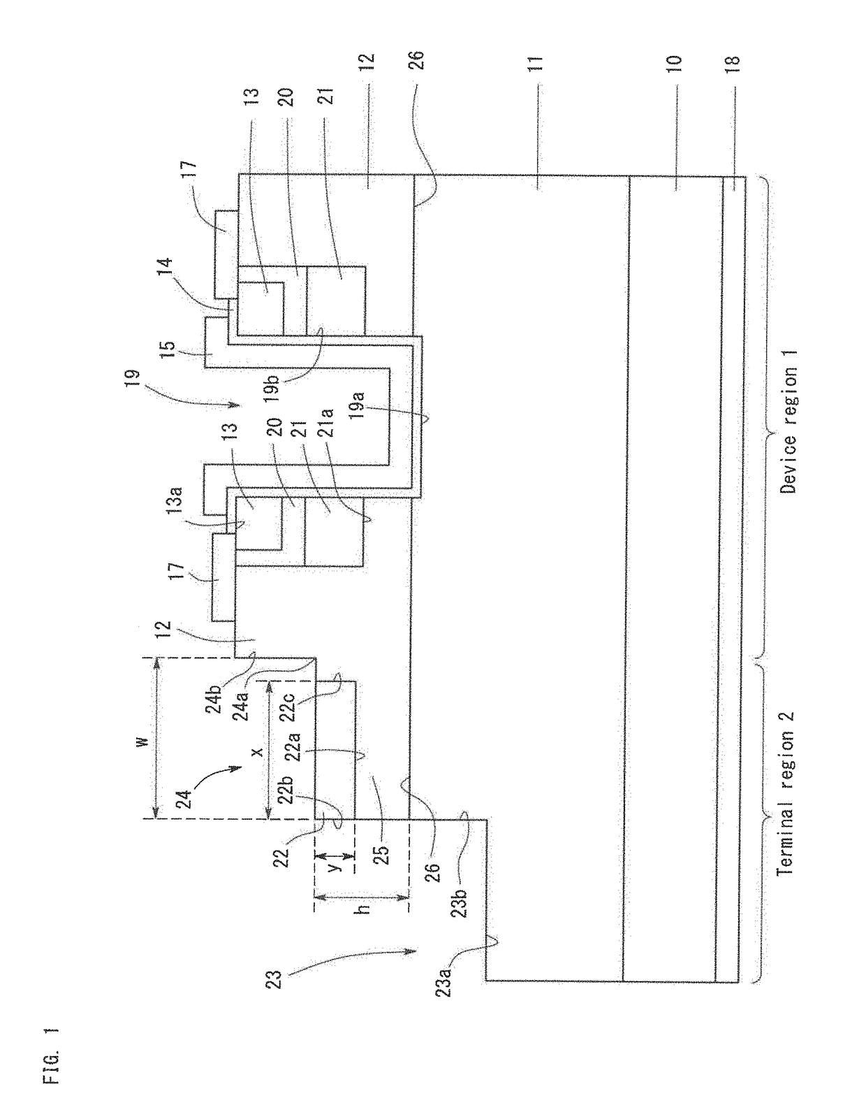
[0087]FIG. 5 is a sketch showing the structure of a semiconductor device according to Embodiment 2. The semiconductor device according to Embodiment 2 has the same structure as the semiconductor device according to Embodiment 1 except for that the gradient distributed low concentration p-type layer region 22 is replaced with the gradient distributed low concentration p-type layer region 222.

[0088]As shown in FIG. 5, the bottom surface 222a where the gradient distributed low concentration p-type layer region 222 is in contact with the p-type layer 12 is closer to the first n-type layer 11 than the bottom surface 21a where the gradient distributed low concentration p-type layer region 21 is in contact with the p-type layer 12 is to the first n-type layer 11. That is, a height difference Δy is provided between the bottom surface 222a of the gradient distributed low concentration p-type layer region 222 and the bottom surface 21a of the gradient distributed low concentration p-type regi...

embodiment 3

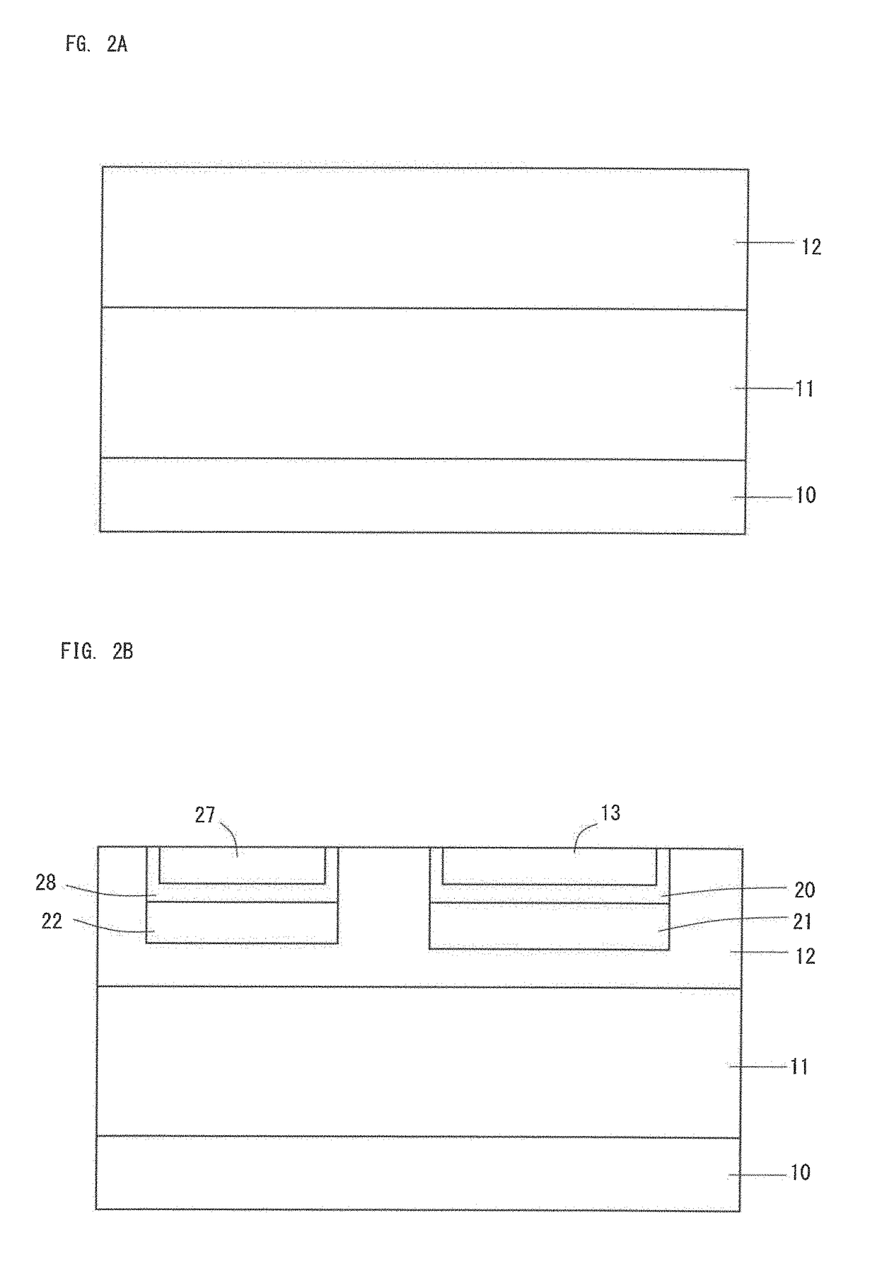
[0090]FIG. 6 is a sketch showing the structure of the semiconductor device according to Embodiment 3. The semiconductor device according to Embodiment 3 has the structure in which the second n-type layer 13 is replaced with the second n-type layer 313, and the low concentration p-type layer region 20 and the gradient distributed low concentration p-type layer region 21 are not formed in the semiconductor device according to Embodiment 1. Other structure is the same as the structure of the semiconductor device according to Embodiment 1.

[0091]The second n-type layer 313 is a layer made of Si-doped n-GaN formed by crystal growth through MOCVD, and obtains an n-type conductivity by supplying a dopant gas in the crystal growth. Since n-GaN is not formed by ion implantation unlike the second n-type layer 13, a low concentration p-type layer region 20 or a gradient distributed low concentration p-type layer region 21 is not formed just below the second n-type layer 313. In other words, onl...


PUM


Abstract

To improve the breakdown voltage of a semiconductor device. In a terminal region of the semiconductor device, a mesa groove, a recess groove, an electric field relaxation region, and a gradient distributed low concentration p-type layer region are formed. A recess groove is fromed between a device region and the mesa groove so as to surround the device region. A region where a p-type layer is thinned by the recess groove is the electric field relaxation region. The gradient distributed low concentration p-type layer region is formed on the surface of the electric field relaxation region. The average carrier concentration of the entire gradient distributed low concentration p-type layer region is lower than the carrier concentration of the p-type layer. By forming the gradient distributed low concentration p-type layer region, the electric field relaxation region is quickly completely depleted when a reverse voltage is applied, thereby improving the breakdown voltage.

Description

BACKGROUND OF THE INVENTIONField of the Invention[0001]The present invention relates to a semiconductor device having a terminal structure in the outer periphery of a device region, and a production method therefor.Background Art[0002]In a vertical semiconductor device establishing electrical continuity in a direction perpendicular to the main surface of a substrate, a pn junction interface is exposed on a terminal part of the device. When a reverse voltage is applied to the semiconductor device, there is a problem that the breakdown voltage does not reach the design value because the electric field is concentrated at the pn interface exposed on the terminal surface. A terminal structure such as field plate structure and guard ring structure is generally formed in the outer periphery of the device region to improve the breakdown voltage.[0003]Japanese Patent No. 5691259 discloses the structure in which recess grooves are formed on the terminal region of the p-type layer formed on th...

Claims


Application Information

Patent Timeline
Patent Type & Authority Applications(United States)
IPC IPC(8): H01L29/78H01L29/66H01L29/06H01L29/10H01L21/265H01L29/40H01L29/20H01L29/08
CPCH01L29/7813H01L29/2003H01L29/66734H01L29/0882H01L29/0619H01L29/1095H01L21/2654H01L29/402H01L29/0865H01L29/7811H01L29/0615H01L29/0661
Inventor UENO, YUKIHISATANAKA, NARIAKI
Owner TOYODA GOSEI CO LTD
Why Eureka
Try Eureka